- 您現在的位置:買賣IC網 > PDF目錄374597 > RM3283 (Fairchild Semiconductor Corporation) Dual ARINC 429 Line Receiver PDF資料下載
參數資料
| 型號: | RM3283 |
| 廠商: | Fairchild Semiconductor Corporation |
| 英文描述: | Dual ARINC 429 Line Receiver |
| 中文描述: | 雙的ARINC 429線路接收器 |
| 文件頁數: | 1/10頁 |
| 文件大小: | 144K |
| 代理商: | RM3283 |
www.fairchildsemi.com
REV. 1.0.1 12/7/00
Features
Two separate analog receiver channels
Converts ARINC 429 levels to serial data
Built-in TTL compatible complete channel test inputs
TTL and CMOS compatible outputs
Low power dissipation
Internal bandgap
Short circuit protected
Available in 20-Lead ceramic DIP
Description
The RM3283 consists of two analog ARINC 429 receivers
which take differentially encoded ARINC level data and
convert it to serial TTL level data. The RM3283 provides
two complete analog ARINC receivers and no external
components are required.
Input level shifting thin film resistors and bipolar technology
allow ARINC input voltage transients up to ±100V without
damage to the RM3283.
Each channel is identical, featuring symmetrical propagation
delays for better high speed performance. Input common
mode rejection is excellent and threshold voltage is stable,
independent of supply voltage. Data outputs are TTL and
CMOS compatible.
Two TTL compatible test inputs used to test the ARINC
channels are available. They can be used to override the
ARINC input data and set the channel outputs to a known
state.
The Fairchild RM3182A line driver is the companion chip to
the RM3283 line receiver. Together they provide the analog
functions needed for the ARINC 429 interface. Digital data
processing involving serial-to-parallel conversion and clock
recovery can be accomplished using one of the ARINC
interface IC’s available or by an equivalent gate array
implementation.
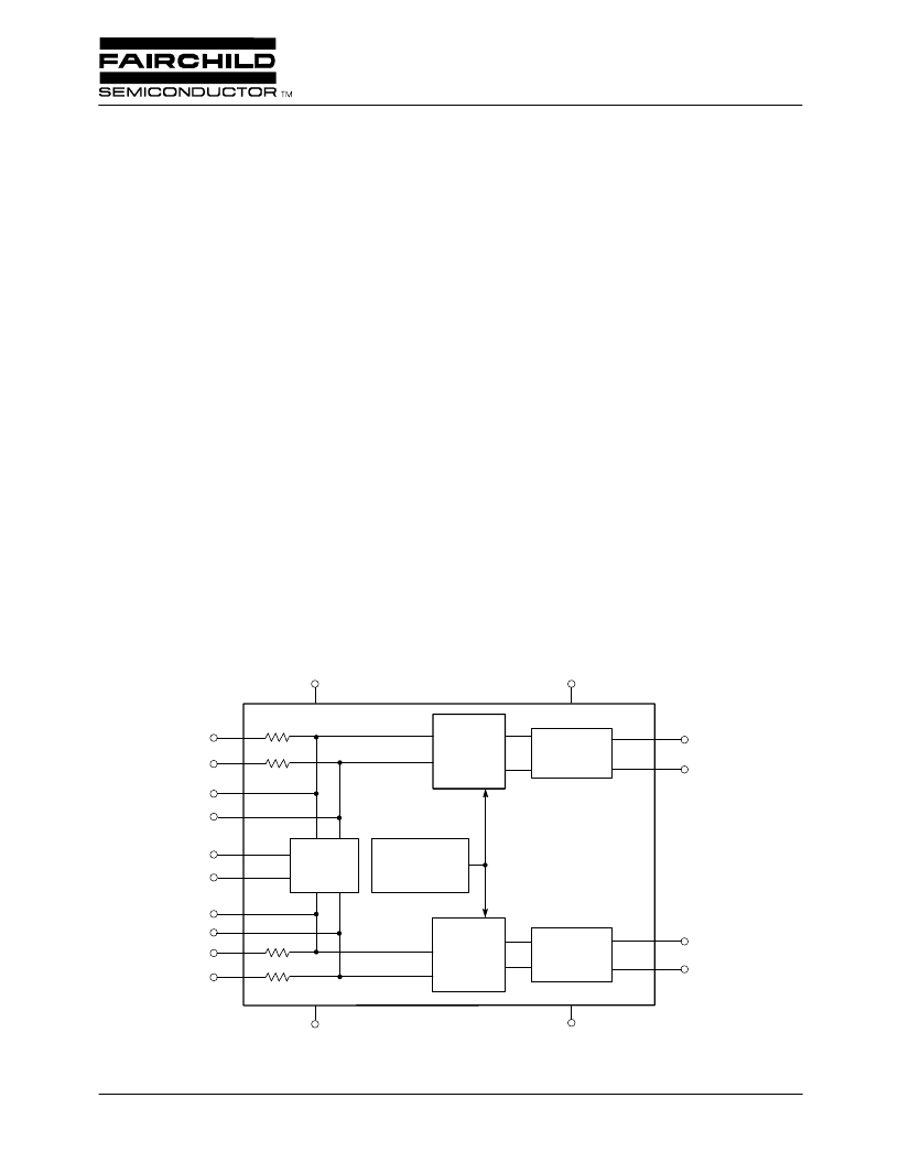
Block Diagram
65-3283-01
-V
S
+V
S
Gnd
+V
L
Bit
Detection
and Level
Shifting
Hysteresis
Channel
Test
Circuitry
Bit Detection
and Level
Shifting
Hysteresis
Out 1A
Out 1B
Out 2A
Out 2B
In 1A
In 1B
Cap 1A
Cap 1B
Test A
Test B
In 2A
In 2B
Cap 2A
Cap 2B
18
16
19
17
2
20
6
4
7
3
1
14
11
9
15
12
8
5
Output
Driver
Output
Driver
Bandgap Voltage
Reference
Threshold
Generator
RM3283
RM3283
Dual ARINC 429 Line Receiver
相關PDF資料 |
PDF描述 |
|---|---|
| RM3283D | Dual ARINC 429 Line Receiver |
| RM35HG-34S | Super Fast Recovery Diodes |
| RM35HG-34S | Super Fast Recovery Single Diode (35 Amperes/1700 Volts) |
| RM400DY-66S | HIGH POWER, HIGH SPEED SWITCHING USE INSULATED TYPE |
| RM400HA-24S | HIGH SPEED SWITCHING USE INSULATED TYPE |
相關代理商/技術參數 |
參數描述 |
|---|---|
| RM3283D | 制造商:FAIRCHILD 制造商全稱:Fairchild Semiconductor 功能描述:Dual ARINC 429 Line Receiver |
| RM3283L | 制造商:未知廠家 制造商全稱:未知廠家 功能描述:Line Receiver |
| RM328-R2 | 制造商:Black Box Corporation 功能描述:Panhead Screws, 10-32, 1 1/8", , 20-Pack 制造商:Black Box Corporation 功能描述:RELAY RACK CUP HEAD SCREWS - 20PC, 10/32 |
| RM329 | 制造商:Black Box Corporation 功能描述:MULTI-BAY JOINING KIT |
| RM330M | 制造商:未知廠家 制造商全稱:未知廠家 功能描述:R. F. Molded Chokes |
發布緊急采購,3分鐘左右您將得到回復。