- 您現(xiàn)在的位置:買賣IC網(wǎng) > PDF目錄26872 > SFH615A-4-X001 (VISHAY INTERTECHNOLOGY INC) 1 CHANNEL TRANSISTOR OUTPUT OPTOCOUPLER PDF資料下載
參數(shù)資料
| 型號(hào): | SFH615A-4-X001 |
| 廠商: | VISHAY INTERTECHNOLOGY INC |
| 元件分類: | 光電耦合器 |
| 英文描述: | 1 CHANNEL TRANSISTOR OUTPUT OPTOCOUPLER |
| 封裝: | PLASTIC, DIP-4 |
| 文件頁數(shù): | 1/3頁 |
| 文件大小: | 387K |
| 代理商: | SFH615A-4-X001 |
Document Number: 83671
www.vishay.com
Revision 17-August-01
2–236
SFH615A
5.3 kV
TRIOS Optocoupler
High Reliability
FEATURES
Variety of Current Transfer Ratios at IF=10 mA
– SFH615A-1, 40–80%
– SFH615A-2, 63–125%
– SFH615A-3, 100–200%
– SFH615A-4, 160–320%
Low CTR Degradation
Good CTR Linearity Depending on Forward
Current
Withstand Test Voltage, 5300 VRMS
High Collector-Emitter Voltage, VCEO=70 V
Low Saturation Voltage
Fast Switching Times
Field-Effect Stable by TRIOS
(TRansparent IOn Shield)
Temperature Stable
Low Coupling Capacitance
End-Stackable, .100" (2.54 mm) Spacing
High Common-Mode Interference Immunity
(Unconnected Base)
Underwriters Lab File #52744
VDE 0884 Available with Option 1
DESCRIPTION
The SFH615A features a large variety of transfer ratio,
low coupling capacitance and high isolation voltage.
These couplers have a GaAs infrared emitting diode
emitter, which is optically coupled to a silicon planar
phototransistor detector, and is incorporated in a plas-
tic DIP-4 package.
The coupling devices are designed for signal transmis-
sion between two electrically separated circuits.
The couplers are end-stackable with 2.54 mm lead
spacing.
Creepage and clearance distances of >8.0 mm are
achieved with option 6. This version complies with IEC
950 (DIN VDE 0805) for reinforced insulation up to an
operation voltage of 400 VRMS or DC.
Specications subject to change.
V
DE
Maximum Ratings
Emitter
Reverse Voltage ...............................................................................6.0 V
DC Forward Current ...................................................................... 60 mA
Surge Forward Current (tP≤10 s) ....................................................2.5 A
Total Power Dissipation .............................................................. 100 mW
Detector
Collector-Emitter Voltage...................................................................70 V
Emitter-Collector Voltage..................................................................7.0 V
Collector Current ........................................................................... 50 mA
Collector Current (tP≤1.0 ms) ...................................................... 100 mA
Total Power Dissipation .............................................................. 150 mW
Package
Isolation Test Voltage between Emitter and
Detector, refer to Climate DIN 40046,
part 2, Nov. 74, t=1.0 s ....................................................... 5300 VRMS
Creepage ....................................................................................
≥7.0 mm
Clearance....................................................................................
≥7.0 mm
Insulation Thickness between Emitter and Detector .................
≥0.4 mm
Comparative Tracking Index
per DIN IEC 112/VDE0 303, part 1................................................
≥175
Isolation Resistance
VIO=500 V, TA=25°C ................................................................ ≥10
12
VIO=500 V, TA=100°C .............................................................. ≥10
11
Storage Temperature Range..............................................–55 to +150
°C
Ambient Temperature Range ............................................–55 to +100
°C
Junction Temperature..................................................................... 100
°C
Soldering Temperature (max. 10 s. Dip Soldering
Distance to Seating Plane
≥1.5 mm) .......................................... 260°C
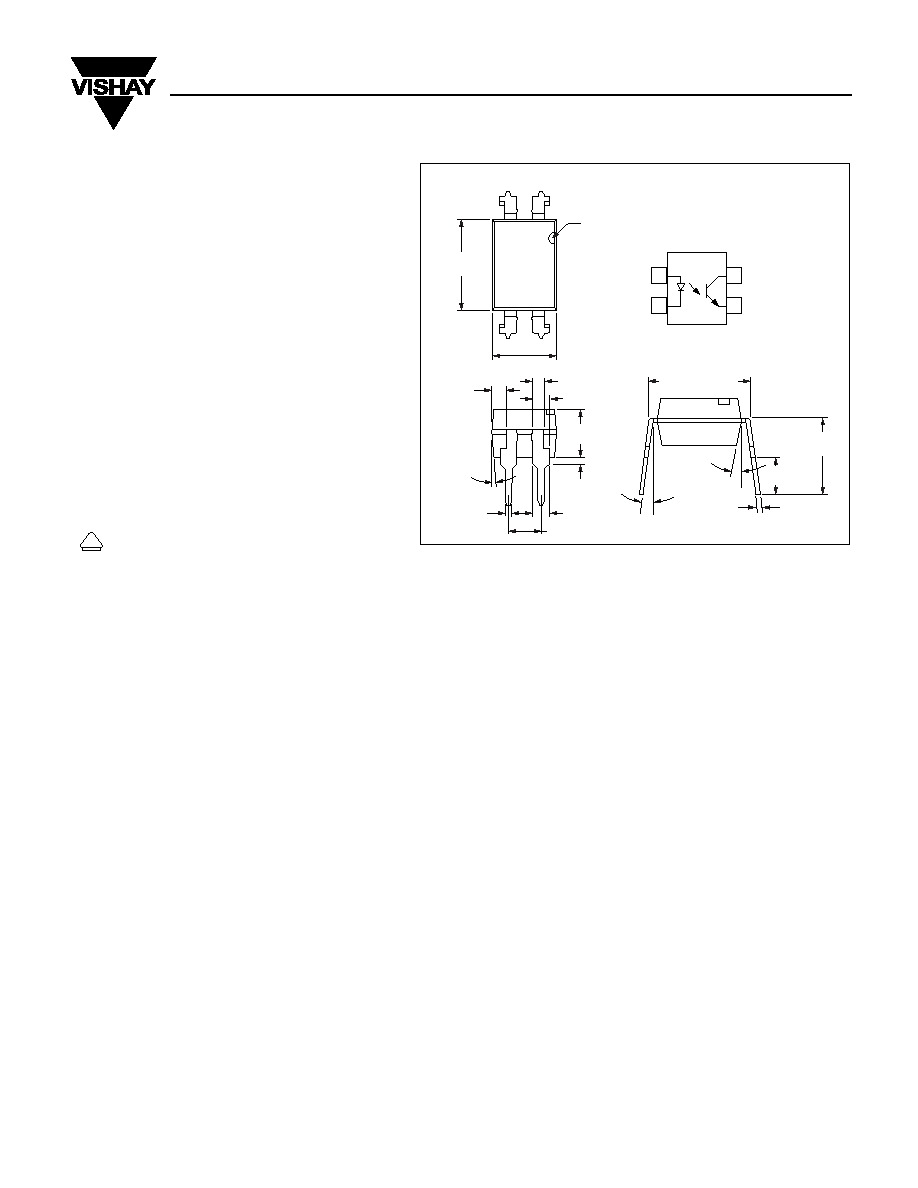
.255 (6.48)
.268 (6.81)
1
2
4
3
.179 (4.55)
.190 (4.83)
pin one ID
.030 (.76)
.045 (1.14)
4
°
typ.
0.100 (2.54)
.130 (3.30)
.150 (3.81)
.020 (.508 )
.035 (.89)
10
°
3
°–9°
.018 (.46)
.022 (.56)
.008 (.20)
.012 (.30)
.031 (.79) typ.
.050 (1.27) typ.
.300 (7.62) typ.
.110 (2.79)
.130 (3.30)
.230 (5.84)
.250 (6.35)
.050 (1.27)
Dimensions in inches (mm)
1
2
4
3
Anode
Collector
Cathode
Emitter
相關(guān)PDF資料 |
PDF描述 |
|---|---|
| SFH615A-4-X009 | 1 CHANNEL TRANSISTOR OUTPUT OPTOCOUPLER |
| SFH615A-2-X006 | 1 CHANNEL TRANSISTOR OUTPUT OPTOCOUPLER |
| SFH615A-1-X006 | 1 CHANNEL TRANSISTOR OUTPUT OPTOCOUPLER |
| SFH615A-4XG | 1 CHANNEL TRANSISTOR OUTPUT OPTOCOUPLER |
| SFH615A-4SMT&R | 1 CHANNEL TRANSISTOR OUTPUT OPTOCOUPLER |
相關(guān)代理商/技術(shù)參數(shù) |
參數(shù)描述 |
|---|---|
| SFH615A-4X006 | 制造商:VISHAY 制造商全稱:Vishay Siliconix 功能描述:Optocoupler, High Reliability, 5300 VRMS |
| SFH615A-4X007 | 制造商:VISHAY 制造商全稱:Vishay Siliconix 功能描述:Optocoupler, Phototransistor Output, High Reliability, 5300 VRMS |
| SFH615A-4X008 | 制造商:VISHAY 制造商全稱:Vishay Siliconix 功能描述:Optocoupler, High Reliability, 5300 VRMS |
| SFH615A-4X008T | 功能描述:晶體管輸出光電耦合器 Phototransistor Out Single CTR>160-320% RoHS:否 制造商:Vishay Semiconductors 輸入類型:DC 最大集電極/發(fā)射極電壓:70 V 最大集電極/發(fā)射極飽和電壓:0.4 V 絕緣電壓:5300 Vrms 電流傳遞比:100 % to 200 % 最大正向二極管電壓:1.65 V 最大輸入二極管電流:60 mA 最大集電極電流:100 mA 最大功率耗散:100 mW 最大工作溫度:+ 110 C 最小工作溫度:- 55 C 封裝 / 箱體:DIP-4 封裝:Bulk |
| SFH615A-4X009 | 功能描述:晶體管輸出光電耦合器 Phototransistor Out Single CTR>160-320% RoHS:否 制造商:Vishay Semiconductors 輸入類型:DC 最大集電極/發(fā)射極電壓:70 V 最大集電極/發(fā)射極飽和電壓:0.4 V 絕緣電壓:5300 Vrms 電流傳遞比:100 % to 200 % 最大正向二極管電壓:1.65 V 最大輸入二極管電流:60 mA 最大集電極電流:100 mA 最大功率耗散:100 mW 最大工作溫度:+ 110 C 最小工作溫度:- 55 C 封裝 / 箱體:DIP-4 封裝:Bulk |
發(fā)布緊急采購,3分鐘左右您將得到回復(fù)。