- 您現(xiàn)在的位置:買賣IC網(wǎng) > PDF目錄26873 > SFH619A-X019 (VISHAY SEMICONDUCTORS) 1 CHANNEL DARLINGTON OUTPUT OPTOCOUPLER PDF資料下載
參數(shù)資料
| 型號(hào): | SFH619A-X019 |
| 廠商: | VISHAY SEMICONDUCTORS |
| 元件分類: | 光電耦合器 |
| 英文描述: | 1 CHANNEL DARLINGTON OUTPUT OPTOCOUPLER |
| 封裝: | ROHS COMPLIANT, SMD, 4 PIN |
| 文件頁數(shù): | 6/13頁 |
| 文件大小: | 241K |
| 代理商: | SFH619A-X019 |
www.vishay.com
For technical questions, contact: optocoupler.answers@vishay.com
Document Number: 83674
2
Rev. 1.7, 15-Feb-11
SFH619A
Vishay Semiconductors
Optocoupler, Photodarlington
Output, High Gain, 300 V BVCEO
Notes
Stresses in excess of the absolute maximum ratings can cause permanent damage to the device. Functional operation of the device is not
implied at these or any other conditions in excess of those given in the operational sections of this document. Exposure to absolute
maximum ratings for extended periods of the time can adversely affect reliability.
(1) Refer to reflow profile for soldering conditions for surface mounted devices (SMD). Refer to wave profile for soldering conditions for through
hole devices (DIP).
Note
Minimum and maximum values are testing requirements. Typical values are characteristics of the device and are the result of engineering
evaluation. Typical values are for information only and are not part of the testing requirements.
COUPLER
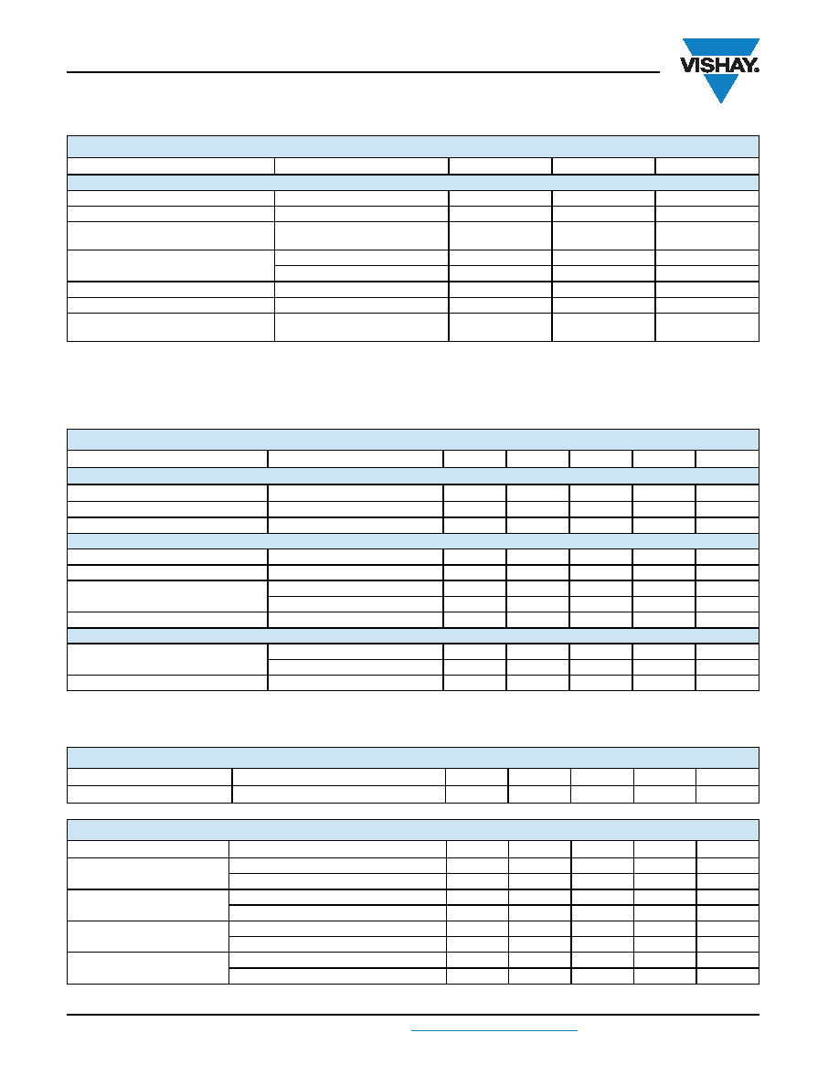
Derate linearly from 25 °C
3.33
mW/°C
Total power dissipation
Ptot
250
mW
Isolation test voltage
between emitter and detector
t = 1 s
VISO
5300
VRMS
Isolation resistance
VIO = 500 V, Tamb = 25 °C
RIO
1012
VIO = 500 V, Tamb = 100 °C
RIO
1011
Storage temperature
Tstg
- 55 to + 150
°C
Operating temperature
Tamb
- 55 to + 100
°C
Soldering temperature (1)
max. 10 s, dip soldering: distance
to seating plane
1.5 mm
Tsld
260
°C
ELECTRICAL CHARACTERISTICS (Tamb = 25 °C, unless otherwise specified)
PARAMETER
TEST CONDITION
SYMBOL
MIN.
TYP.
MAX.
UNIT
INPUT
Forward voltage
IF = 10 mA
VF
1.2
1.5
V
Reverse current
VR = 6 V
IR
0.02
10
μA
Capacitance
VR = 0 V
CO
14
pF
OUTPUT
Collector emitter breakdown voltage
ICE = 100 μA
BVCEO
300
V
Emitter collector breakdown voltage
IEC = 100 μA
BVECO
0.3
V
Collector emitter dark current
VCE = 200 V,TA = 25 °C
ICEO
10
200
nA
VCE = 200 V,TA = 100 °C
ICEO
20
nA
Collector emitter capacitance
VCE = 0 V, f = 1 MHz
CCE
39
pF
COUPLER
Collector emitter saturation voltage
IF = 1 mA, IC = 10 mA
VCEsat
1V
IF = 10 mA, IC = 100 mA
VCEsat
0.3
1.2
V
Coupling capacitance
VI-O = 0 V, f = 1 MHz
CC
0.6
pF
CURRENT TRANSFER RATIO
PARAMETER
TEST CONDITION
SYMBOL
MIN.
TYP.
MAX.
UNIT
Coupling transfer ratio
IF = 1 mA, VCE = 1 V
CTR
1000
%
SWITCHING CHARACTERISTICS
PARAMETER
TEST CONDITION
SYMBOL
MIN.
TYP.
MAX.
UNIT
Rise time
VCC = 10 V, IC = 10 mA, RL = 100
tr
3.5
μs
VCC = 10 V, IF = 16 mA, RL = 180
tr
1μs
Fall time
VCC = 10 V, IC = 10 mA, RL = 100
tf
14.5
μs
VCC = 10 V, IF = 16 mA, RL = 180
tf
20.5
μs
Turn-on time
VCC = 10 V, IC = 10 mA, RL = 100
ton
4.5
μs
VCC = 10 V, IF = 16 mA, RL = 180
ton
1.5
μs
Turn-off time
VCC = 10 V, IC = 10 mA, RL = 100
toff
29
μs
VCC = 10 V, IF = 16 mA, RL = 180
toff
53.5
μs
ABSOLUTE MAXIMUM RATINGS (Tamb = 25 °C, unless otherwise specified)
PARAMETER
TEST CONDITION
SYMBOL
VALUE
UNIT
相關(guān)PDF資料 |
PDF描述 |
|---|---|
| SFH619A | 1 CHANNEL DARLINGTON OUTPUT OPTOCOUPLER |
| SFH620-2G | 1 CHANNEL AC INPUT-TRANSISTOR OUTPUT OPTOCOUPLER |
| SFH628A-4 | 1 CHANNEL AC INPUT-TRANSISTOR OUTPUT OPTOCOUPLER |
| SFH6206-2-X001T | 1 CHANNEL AC INPUT-TRANSISTOR OUTPUT OPTOCOUPLER |
| SFH6116-1-X001 | 1 CHANNEL TRANSISTOR OUTPUT OPTOCOUPLER |
相關(guān)代理商/技術(shù)參數(shù) |
參數(shù)描述 |
|---|---|
| SFH620-1 | 制造商:未知廠家 制造商全稱:未知廠家 功能描述:AC INPUT PHOTOTRANSISTOR OPTICALLY COUPLED ISOLATORS |
| SFH620-1X | 制造商:未知廠家 制造商全稱:未知廠家 功能描述:AC INPUT PHOTOTRANSISTOR OPTICALLY COUPLED ISOLATORS |
| SFH620-2 | 制造商:未知廠家 制造商全稱:未知廠家 功能描述:AC INPUT PHOTOTRANSISTOR OPTICALLY COUPLED ISOLATORS |
| SFH620-2X | 制造商:未知廠家 制造商全稱:未知廠家 功能描述:AC INPUT PHOTOTRANSISTOR OPTICALLY COUPLED ISOLATORS |
| SFH620-3 | 制造商:Vishay Semiconductors 功能描述:OPTOCOUPLER, 4 PIN, CTR 100-320% - Bulk |
發(fā)布緊急采購,3分鐘左右您將得到回復(fù)。