- 您現在的位置:買賣IC網 > PDF目錄385841 > SFH620AA (SIEMENS A G) 5.3 kV TRIOS Optocoupler AC Voltage Input PDF資料下載
參數資料
| 型號: | SFH620AA |
| 廠商: | SIEMENS A G |
| 元件分類: | 光電耦合器 |
| 英文描述: | 5.3 kV TRIOS Optocoupler AC Voltage Input |
| 中文描述: | 1 CHANNEL AC INPUT-TRANSISTOR OUTPUT OPTOCOUPLER |
| 封裝: | PLASTIC, DIP-4 |
| 文件頁數: | 1/3頁 |
| 文件大小: | 73K |
| 代理商: | SFH620AA |
1
Maximum Ratings
Emitter
Reverse Voltage ..............................................................................
Surge Forward Current (t
P
≤
10
μ
s).....................................................
Total Power Dissipation.................................................................. 100 mW
Detector
Collector-Emitter Voltage..................................................................... 70 V
Emitter-Collector Voltage........................................................................ 7 V
Collector Current...............................................................................50 mA
Collector Current (t
P
≤
1 ms) .............................................................100 mA
Total Power Dissipation.................................................................. 150 mW
Package
Isolation Test Voltage between Emitter and
Detector, refer to Climate DIN 40046,
part 2, Nov. 74................................................................... 5300 VAC
Creepage .........................................................................................
Clearance.........................................................................................
Insulation Thickness between Emitter and Detector....................... 0.4 mm
Comparative Tracking Index
per DIN IEC 112/VDE0 303, part 1.................................................... 175
Isolation Resistance
V
IO
=500 V, T
A
=25
°
C ...................................................................
V
IO
=500 V, T
A
=100
°
C .................................................................
Storage Temperature Range................................................ –55 to +150
Ambient Temperature Range ............................................... –55 to +100
J unction Temperature........................................................................ 100
Soldering Temperature (max. 10 s. Dip Soldering
Distance to Seating Plane
≥
1.5 mm) ............................................. 260
±
60 mA
±
2.5 A
RMS
7 mm
≥
7 mm
≥
≥
≥
10
10
12
11
°
°
°
C
C
C
°
C
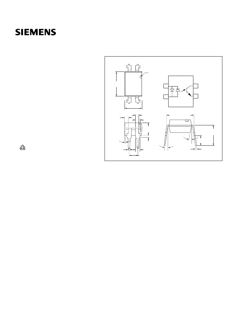
.255 (6.48)
.268 (6.81)
1
2
4
3
.179 (4.55)
.190 (4.83)
pin one ID
.030 (.76)
.045 (1.14)
4
°
typ.
1.00 (2.54)
.130 (3.30)
.150 (3.81)
.020 (.508 )
.035 (.89)
.050 (1.27)
10
°
3
°
–9
.018 (.46)
.022 (.56)
.008 (.20)
.012 (.30)
.031 (.79) typ.
.050 (1.27) typ.
.300 (7.62) typ.
.110 (2.79)
.130 (3.30)
.230 (5.84)
.250 (6.35)
1
2
4
3
Collector
Emitter
Anode/
Cathode
Cathode/
Anode
Dimensions in Inches (mm)
FEATURES
High Current Transfer Ratios
at 5 mA: 50–600%
at 1 mA: 45% typical (>13)
Low CTR Degradation
Good CTR Linearity Depending on Forward
Current
Isolation Test Voltage, 5300 VAC
High Collector-Emitter Voltage, V
Low Saturation Voltage
Fast Switching Times
Field-Effect Stable by TRIOS (TRansparent IOn
Shield)
Temperature Stable
Low Coupling Capacitance
End-Stackable, .100"(2.54 mm) Spacing
High Common-Mode Interference Immunity
(Unconnected Base)
Underwriters Lab File #52744
VDE 0884 Available with Option 1
SMD Option, See SFH6206 Data Sheet
RMS
CEO
=70 V
DESCRIPTION
The SFH620AA/AGB features a high current transfer
ratio, low coupling capacitance and high isolation
voltage. These couplers have a GaAs infrared emit-
ting diode emitter, which is optically coupled to a sil-
icon planar phototransistor detector, and is
incorporated in a plastic DIP-4 package.
The coupling devices are designed for signal trans-
mission between two electrically separated circuits.
The couplers are end-stackable with 2.54 mm spac-
ing.
Creepage and clearance distances of >8 mm are
achieved with option 6. This version complies with
IEC 950 (DIN VDE 0805) for reinforced insulation up
to an operation voltage of 400 V
RMS
or DC.
SFH620AA/AGB
5.3 kV TRIOS
AC Voltage Input
Optocoupler
相關PDF資料 |
PDF描述 |
|---|---|
| SFH620AGB | 5.3 kV TRIOS Optocoupler AC Voltage Input |
| SFH6319T | LOW CURRENT, HIGH GAIN OPTOCOUPLER |
| SFH6319 | LOW CURRENT, HIGH GAIN OPTOCOUPLER |
| SFH6343T | HIGH SPEED OPTOCOUPLER |
| SFS1826 | 1.6 AMPS 200 Α 400 VOLTS SILICON CONTROLLED RECTIFIER |
相關代理商/技術參數 |
參數描述 |
|---|---|
| SFH620AA-X009 | 制造商:VISHAY 制造商全稱:Vishay Siliconix 功能描述:Optocoupler, AC Input, 5300 VRMS |
| SFH620AA-X009T | 功能描述:晶體管輸出光電耦合器 Phototransistor Out AC-In CTR>50-600% RoHS:否 制造商:Vishay Semiconductors 輸入類型:DC 最大集電極/發射極電壓:70 V 最大集電極/發射極飽和電壓:0.4 V 絕緣電壓:5300 Vrms 電流傳遞比:100 % to 200 % 最大正向二極管電壓:1.65 V 最大輸入二極管電流:60 mA 最大集電極電流:100 mA 最大功率耗散:100 mW 最大工作溫度:+ 110 C 最小工作溫度:- 55 C 封裝 / 箱體:DIP-4 封裝:Bulk |
| SFH620AGB | 功能描述:晶體管輸出光電耦合器 Phototransistor Out Single CTR 100-600% RoHS:否 制造商:Vishay Semiconductors 輸入類型:DC 最大集電極/發射極電壓:70 V 最大集電極/發射極飽和電壓:0.4 V 絕緣電壓:5300 Vrms 電流傳遞比:100 % to 200 % 最大正向二極管電壓:1.65 V 最大輸入二極管電流:60 mA 最大集電極電流:100 mA 最大功率耗散:100 mW 最大工作溫度:+ 110 C 最小工作溫度:- 55 C 封裝 / 箱體:DIP-4 封裝:Bulk |
| SFH620AGB-X001 | 制造商:Vishay Angstrohm 功能描述:Optocoupler AC-IN 1-CH Transistor DC-OUT 4-Pin DIP T/R 制造商:Vishay Semiconductors 功能描述:DIP-4 CPLR 100-600% CTR VDE-E3 - Tape and Reel 制造商:Vishay Semiconductors 功能描述:OPTOCOUPLER, PHOTOTRANSISTOR O/P, 5.3KV, DIP-4; No. of Channels:1; Isolation Voltage:5.3kV; Optocoupler Output Type:Phototransistor; Input Current:60mA; Output Voltage:70V; Opto Case Style:DIP; No. of Pins:4 ;RoHS Compliant: Yes |
| SFH620AGB-X007 | 制造商:VISHAY 制造商全稱:Vishay Siliconix 功能描述:Optocoupler, AC Input, 5300 VRMS |
發布緊急采購,3分鐘左右您將得到回復。