- 您現在的位置:買賣IC網 > PDF目錄8721 > SL2309ZC-1H (Silicon Laboratories Inc)IC BUFFER 140MHZ 9CH3.3V 16TSSOP PDF資料下載
參數資料
| 型號: | SL2309ZC-1H |
| 廠商: | Silicon Laboratories Inc |
| 文件頁數: | 1/12頁 |
| 文件大小: | 0K |
| 描述: | IC BUFFER 140MHZ 9CH3.3V 16TSSOP |
| 標準包裝: | 96 |
| 系列: | EProClock® |
| 類型: | * |
| PLL: | 帶旁路 |
| 輸入: | 時鐘 |
| 輸出: | 時鐘 |
| 電路數: | 1 |
| 比率 - 輸入:輸出: | 1:9 |
| 差分 - 輸入:輸出: | 無/無 |
| 頻率 - 最大: | 140MHz |
| 除法器/乘法器: | 無/無 |
| 電源電壓: | 3 V ~ 3.6 V |
| 工作溫度: | 0°C ~ 70°C |
| 安裝類型: | * |
| 封裝/外殼: | * |
| 供應商設備封裝: | * |
| 包裝: | * |
Rev 1.3, July 31, 2007
Page 1 of 12
400 West Cesar Chavez, Austin, TX 78701
1+(512) 416-8500
1+(512) 416-9669
www.silabs.com
SL2309
Key Features
10 to 140 MHz operating frequency range
Low output clock jitter:
140 ps-max cycle-to-cycle jitter
Low output-to-output skew: 150 ps-max
Low product-to-product skew: 400 ps-max
3.3 V power supply range
Low power dissipation:
26 mA-max at 66 MHz
44 mA –max at 133 MHz
One input drives 9 outputs organized as 4+4+1
Select mode to bypass PLL or tri-state outputs
SpreadThru PLL that allows use of SSCG
Standard and High-Drive options
Available in 16-pin SOIC and TSSOP packages
Available in Commercial and Industrial grades
Applications
Printers and MFPs
Digital Copiers
PCs and Work Stations
DTV
Routers, Switchers and Servers
Digital Embeded Systems
Description
The SL2309 is a low skew, low jitter and low power Zero
Delay Buffer (ZDB) designed to produce up to nine (9)
clock outputs from one (1) reference input clock, for high
speed clock distribution applications.
The product has an on-chip PLL which locks to the input
clock at CLKIN and receives its feedback internally from
the CLKOUT pin.
The SL2309 has two (2) clock driver banks each with four
(4) clock outputs. These outputs are controlled by two (2)
select input pins S1 and S2. When only four (4) outputs
are needed, four (4) bank-B output clock buffers can be tri-
stated to reduce power dissipation and jitter. The select
inputs can also be used to tri-state both banks A and B or
drive them directly from the input bypassing the PLL and
making the product behave like a Non-Zero Delay Fanout
Buffer (NZDB).
The high-drive (-1H) version operates up to 140MHz and
low drive (-1) version operates up to 100MHz at 3.3V.
Benefits
Up to nine (9) distribution of input clock
Standard and High-Drive levels to control impedance
level, frequency range and EMI
Low power dissipation, jitter and skew
Low cost
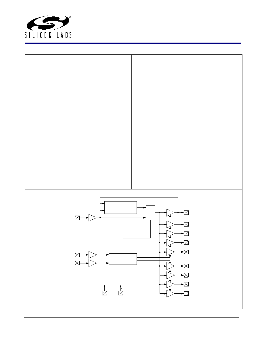
Block Diagram
Low Power and
Low Jitter
PLL
MUX
Input Selection
Decoding Logic
VDD
GND
2
S2
S1
CLKIN
CLKOUT
CLKA1
CLKA2
CLKA3
CLKA4
CLKB1
CLKB2
CLKB3
CLKB4
Low Jitter and Skew 10 to 140 MHz Zero Delay Buffer (ZDB)
相關PDF資料 |
PDF描述 |
|---|---|
| SL2305SI-1HT | IC BUFFER 140MHZ 5CH 3.3V 8SOIC |
| SL2305ZI-1H | IC BUFFER 140MHZ 5CH 3.3V 8TSSOP |
| SL2305SI-1H | IC BUFFER 140MHZ 5CH 3.3V 8SOIC |
| SL23EP09ZC-1T | IC BUFFER 220MHZ 9CH3.3V 16TSSOP |
| VE-231-MW-F1 | CONVERTER MOD DC/DC 12V 100W |
相關代理商/技術參數 |
參數描述 |
|---|---|
| SL2309ZC-1HT | 功能描述:時鐘緩沖器 10-140MHz 9 Outputs ZDB 3.3V High Drive RoHS:否 制造商:Texas Instruments 輸出端數量:5 最大輸入頻率:40 MHz 傳播延遲(最大值): 電源電壓-最大:3.45 V 電源電壓-最小:2.375 V 最大功率耗散: 最大工作溫度:+ 85 C 最小工作溫度:- 40 C 封裝 / 箱體:LLP-24 封裝:Reel |
| SL2309ZC-1T | 功能描述:時鐘緩沖器 10-140MHz 9 Outputs ZDB 3.3V RoHS:否 制造商:Texas Instruments 輸出端數量:5 最大輸入頻率:40 MHz 傳播延遲(最大值): 電源電壓-最大:3.45 V 電源電壓-最小:2.375 V 最大功率耗散: 最大工作溫度:+ 85 C 最小工作溫度:- 40 C 封裝 / 箱體:LLP-24 封裝:Reel |
| SL2309ZI-1 | 功能描述:時鐘緩沖器 10-140MHz 9 Outputs ZDB 3.3V RoHS:否 制造商:Texas Instruments 輸出端數量:5 最大輸入頻率:40 MHz 傳播延遲(最大值): 電源電壓-最大:3.45 V 電源電壓-最小:2.375 V 最大功率耗散: 最大工作溫度:+ 85 C 最小工作溫度:- 40 C 封裝 / 箱體:LLP-24 封裝:Reel |
| SL2309ZI-1H | 功能描述:時鐘緩沖器 10-140MHz 9 Outputs ZDB 3.3V High Drive RoHS:否 制造商:Texas Instruments 輸出端數量:5 最大輸入頻率:40 MHz 傳播延遲(最大值): 電源電壓-最大:3.45 V 電源電壓-最小:2.375 V 最大功率耗散: 最大工作溫度:+ 85 C 最小工作溫度:- 40 C 封裝 / 箱體:LLP-24 封裝:Reel |
| SL2309ZI-1HT | 功能描述:時鐘緩沖器 10-140MHz 9 Outputs ZDB 3.3V High Drive RoHS:否 制造商:Texas Instruments 輸出端數量:5 最大輸入頻率:40 MHz 傳播延遲(最大值): 電源電壓-最大:3.45 V 電源電壓-最小:2.375 V 最大功率耗散: 最大工作溫度:+ 85 C 最小工作溫度:- 40 C 封裝 / 箱體:LLP-24 封裝:Reel |
發布緊急采購,3分鐘左右您將得到回復。