- 您現在的位置:買賣IC網 > PDF目錄98107 > SN74AVC16501DGG (TEXAS INSTRUMENTS INC) AVC SERIES, 18-BIT REGISTERED TRANSCEIVER, TRUE OUTPUT, PDSO56 PDF資料下載
參數資料
| 型號: | SN74AVC16501DGG |
| 廠商: | TEXAS INSTRUMENTS INC |
| 元件分類: | 總線收發器 |
| 英文描述: | AVC SERIES, 18-BIT REGISTERED TRANSCEIVER, TRUE OUTPUT, PDSO56 |
| 封裝: | PLASTIC, TSSOP-56 |
| 文件頁數: | 1/12頁 |
| 文件大小: | 173K |
| 代理商: | SN74AVC16501DGG |
Please be aware that an important notice concerning availability, standard warranty, and use in critical applications of
Texas Instruments semiconductor products and disclaimers thereto appears at the end of this data sheet.
SN74AVC16501
18-BIT UNIVERSAL BUS TRANSCEIVER
WITH 3-STATE OUTPUTS
SCES160D – DECEMBER 1998 – REVISED DECEMBER 1999
1
POST OFFICE BOX 655303
DALLAS, TEXAS 75265
D Member of the Texas Instruments
Widebus
Family
D EPIC (Enhanced-Performance Implanted
CMOS) Submicron Process
D UBT (Universal Bus Transceiver)
Combines D-Type Latches and D-Type
Flip-Flops for Operation in Transparent,
Latched, or Clocked Mode
D DOC (Dynamic Output Control) Circuit
Dynamically Changes Output Impedance,
Resulting in Noise Reduction Without
Speed Degradation
D Dynamic Drive Capability Is Equivalent to
Standard Outputs With IOH and IOL of
±24 mA at 2.5-V VCC
D Overvoltage-Tolerant Inputs/Outputs Allow
Mixed-Voltage-Mode Data Communications
D Ioff Supports Partial-Power-Down Mode
Operation
D Package Options Include Plastic Thin
Shrink Small-Outline (DGG) and Thin Very
Small-Outline (DGV) Packages
description
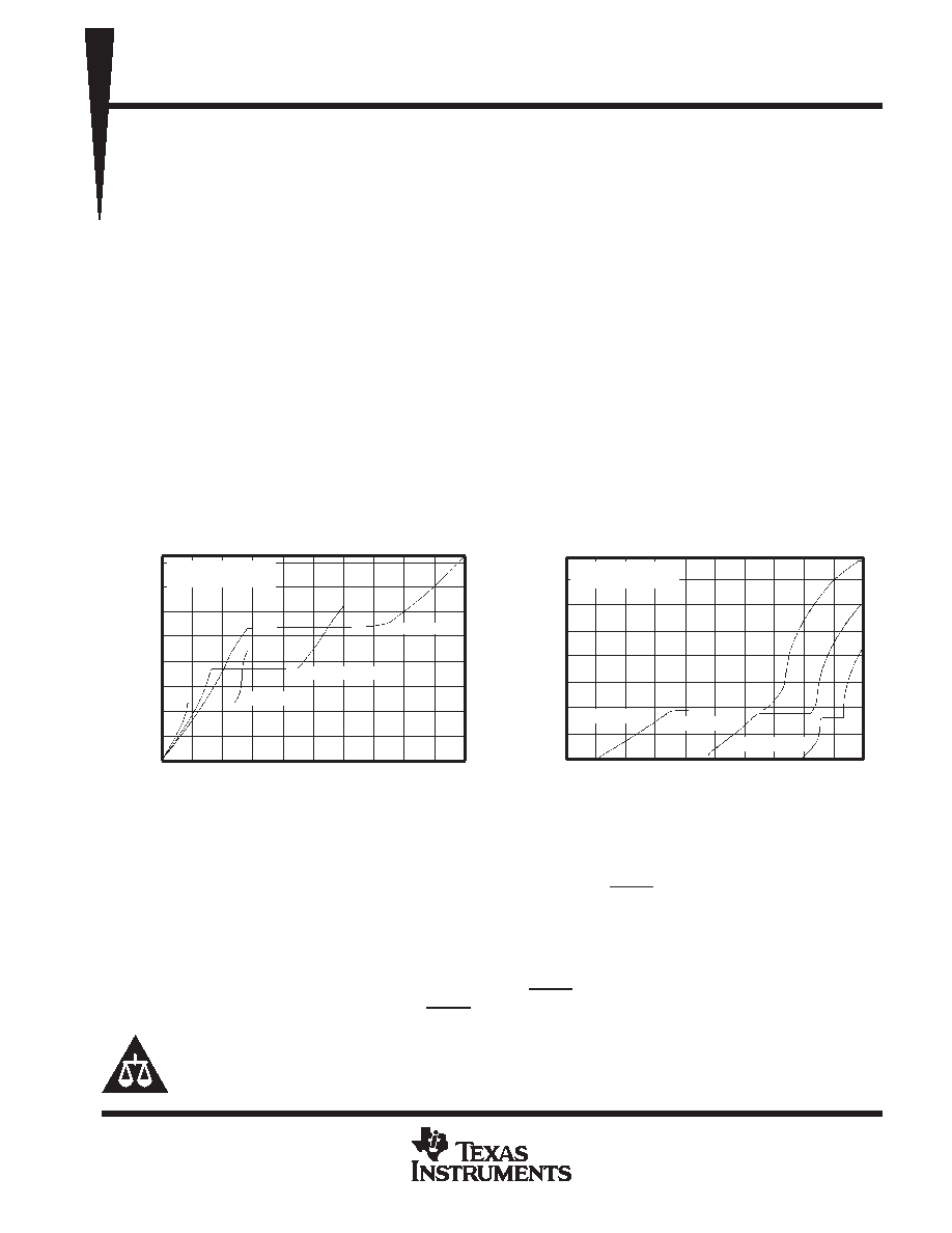
A Dynamic Output Control (DOC) circuit is implemented, which, during the transition, initially lowers the output
impedance to effectively drive the load and, subsequently, raises the impedance to reduce noise. Figure 1
shows typical VOL vs IOL and VOH vs IOH curves to illustrate the output impedance and drive capability of the
circuit. At the beginning of the signal transition, the DOC circuit provides a maximum dynamic drive that is
equivalent to a high-drive standard-output device. For more information, refer to the TI application reports,
AVC
Logic Family Technology and Applications, literature number SCEA006, and Dynamic Output Control (DOC
)
Circuitry Technology and Applications, literature number SCEA009.
3.2
2.8
2.4
2.0
1.6
1.2
0.8
0.4
153
136
119
102
85
68
51
34
17
TA = 25°C
Process = Nominal
IOL – Output Current – mA
VCC = 3.3 V
VCC = 2.5 V
VCC = 1.8 V
–
Output
V
oltage
–
V
OL
V
2.8
2.4
2.0
1.6
1.2
0.8
0.4
–32
–48
–64
–80
–96
–112
–128
–144
–16
TA = 25°C
Process = Nominal
IOH – Output Current – mA
VCC = 3.3 V
VCC = 2.5 V
VCC = 1.8 V
–
Output
V
oltage
–
V
OH
V
170
0
–160
Figure 1. Output Voltage vs Output Current
This 18-bit universal bus transceiver is operational at 1.2-V to 3.6-V VCC, but is designed specifically for 1.65-V
to 3.6-V VCC operation.
Data flow in each direction is controlled by output-enable (OEAB and OEBA), latch-enable (LEAB and LEBA),
and clock (CLKAB and CLKBA) inputs. For A-to-B data flow, the device operates in the transparent mode when
LEAB is high. When LEAB is low, the A data is latched if CLKAB is held at a high or low logic level. If LEAB is
low, the A data is stored in the latch/flip-flop on the low-to-high transition of CLKAB. When OEAB is high, the
outputs are active. When OEAB is low, the outputs are in the high-impedance state.
Data flow for B to A is similar to that of A to B, but uses OEBA, LEBA, and CLKBA. The output enables are
complementary (OEAB is active high and OEBA is active low).
PRODUCT
PREVIEW
PRODUCT PREVIEW information concerns products in the formative or
design phase of development. Characteristic data and other
specifications are design goals. Texas Instruments reserves the right to
change or discontinue these products without notice.
Copyright
1999, Texas Instruments Incorporated
DOC, EPIC, UBT, and Widebus are trademarks of Texas Instruments Incorporated.
相關PDF資料 |
PDF描述 |
|---|---|
| SN74AVC16501DGV | AVC SERIES, 18-BIT REGISTERED TRANSCEIVER, TRUE OUTPUT, PDSO56 |
| SN74AVC16601DGGR | AVC SERIES, 18-BIT REGISTERED TRANSCEIVER, TRUE OUTPUT, PDSO56 |
| SN74AVC16601DGG | AVC SERIES, 18-BIT REGISTERED TRANSCEIVER, TRUE OUTPUT, PDSO56 |
| SN74AVC16646DGGE4 | AVC SERIES, DUAL 8-BIT REGISTERED TRANSCEIVER, TRUE OUTPUT, PDSO56 |
| SN74AVC16827DGGE4 | AVC SERIES, DUAL 10-BIT DRIVER, TRUE OUTPUT, PDSO56 |
相關代理商/技術參數 |
參數描述 |
|---|---|
| SN74AVC16646D | 制造商:Rochester Electronics LLC 功能描述:- Bulk |
| SN74AVC16646DGG | 制造商:Rochester Electronics LLC 功能描述:- Bulk |
| SN74AVC16646DGGR | 功能描述:總線收發器 16bit Bus RoHS:否 制造商:Fairchild Semiconductor 邏輯類型:CMOS 邏輯系列:74VCX 每芯片的通道數量:16 輸入電平:CMOS 輸出電平:CMOS 輸出類型:3-State 高電平輸出電流:- 24 mA 低電平輸出電流:24 mA 傳播延遲時間:6.2 ns 電源電壓-最大:2.7 V, 3.6 V 電源電壓-最小:1.65 V, 2.3 V 最大工作溫度:+ 85 C 封裝 / 箱體:TSSOP-48 封裝:Reel |
| SN74AVC16646DGVR | 功能描述:總線收發器 16bit Bus RoHS:否 制造商:Fairchild Semiconductor 邏輯類型:CMOS 邏輯系列:74VCX 每芯片的通道數量:16 輸入電平:CMOS 輸出電平:CMOS 輸出類型:3-State 高電平輸出電流:- 24 mA 低電平輸出電流:24 mA 傳播延遲時間:6.2 ns 電源電壓-最大:2.7 V, 3.6 V 電源電壓-最小:1.65 V, 2.3 V 最大工作溫度:+ 85 C 封裝 / 箱體:TSSOP-48 封裝:Reel |
| SN74AVC16722DGGR | 功能描述:觸發器 22bit RoHS:否 制造商:Texas Instruments 電路數量:2 邏輯系列:SN74 邏輯類型:D-Type Flip-Flop 極性:Inverting, Non-Inverting 輸入類型:CMOS 輸出類型: 傳播延遲時間:4.4 ns 高電平輸出電流:- 16 mA 低電平輸出電流:16 mA 電源電壓-最大:5.5 V 最大工作溫度:+ 85 C 安裝風格:SMD/SMT 封裝 / 箱體:X2SON-8 封裝:Reel |
發布緊急采購,3分鐘左右您將得到回復。