- 您現在的位置:買賣IC網 > PDF目錄98109 > SN74CB3T3306DCTR (TEXAS INSTRUMENTS INC) CB3T/3VT SERIES, DUAL 1-BIT DRIVER, TRUE OUTPUT, PDSO8 PDF資料下載
參數資料
| 型號: | SN74CB3T3306DCTR |
| 廠商: | TEXAS INSTRUMENTS INC |
| 元件分類: | 總線收發器 |
| 英文描述: | CB3T/3VT SERIES, DUAL 1-BIT DRIVER, TRUE OUTPUT, PDSO8 |
| 封裝: | GREEN, PLASTIC, SSOP-8 |
| 文件頁數: | 1/14頁 |
| 文件大小: | 463K |
| 代理商: | SN74CB3T3306DCTR |
www.ti.com
FEATURES
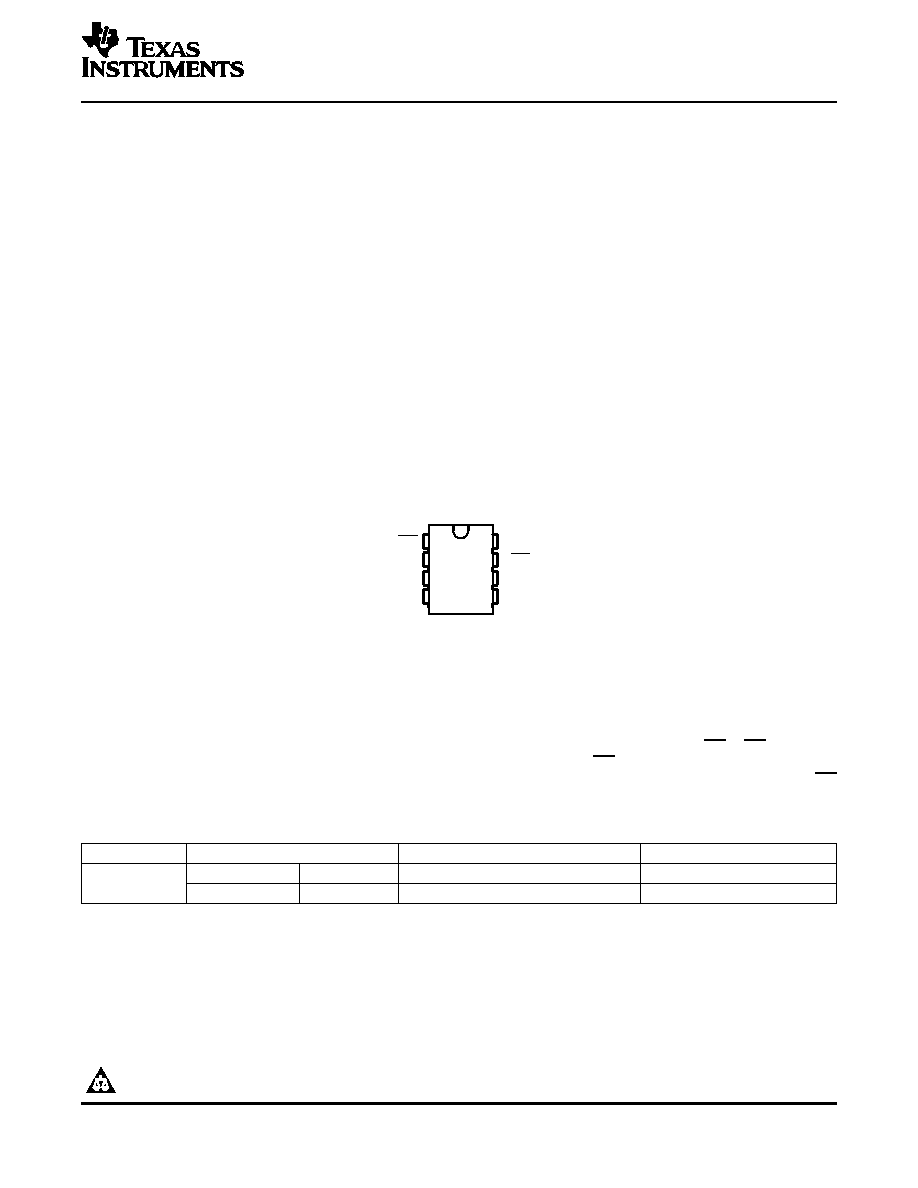
DCT OR DCU PACKAGE
(TOP VIEW)
1
2
3
4
8
7
6
5
1OE
1A
1B
GND
VCC
2OE
2B
2A
DESCRIPTION/ORDERING INFORMATION
SN74CB3T3306
DUAL FET BUS SWITCH 2.5-V/3.3-V LOW-VOLTAGE BUS SWITCH
WITH 5-V TOLERANT LEVEL SHIFTER
SCDS119A – JANUARY 2003 – REVISED JUNE 2005
Low Power Consumption
(ICC = 20 A Max)
Output Voltage Translation Tracks VCC
VCC Operating Range From 2.3 V to 3.6 V
Supports Mixed-Mode Signal Operation
on All Data I/O Ports
Data I/Os Support 0- to 5-V Signaling Levels
(0.8 V, 1.2 V, 1.5 V, 1.8 V, 2.5 V, 3.3 V, 5 V)
– 5-V Input Down to 3.3-V Output Level
Shift With 3.3-V VCC
Control Inputs Can Be Driven by TTL or
5-V/3.3-V CMOS Outputs
– 5-V/3.3-V Input Down to 2.5-V Output
Level Shift With 2.5-V VCC
Ioff Supports Partial-Power-Down Mode
Operation
5-V Tolerant I/Os With Device Powered Up
or Powered Down
Latch-Up Performance Exceeds 250 mA Per
JESD 17
Bidirectional Data Flow With Near-Zero
Propagation Delay
ESD Performance Tested Per JESD 22
Low ON-State Resistance (ron)
– 2000-V Human-Body Model
Characteristics (ron = 5 Typ)
(A114-B, Class II)
Low Input/Output Capacitance Minimizes
– 1000-V Charged-Device Model (C101)
Loading (Cio(OFF) = 4.5 pF Typ)
Supports Digital Applications: Level
Data and Control Inputs Provide
Translation, USB Interface, Bus Isolation
Undershoot Clamp Diodes
Ideal for Low-Power Portable Equipment
The SN74CB3T3306 is a high-speed TTL-compatible FET bus switch with low ON-state resistance (ron), allowing
for minimal propagation delay. The device fully supports mixed-mode signal operation on all data I/O ports by
providing voltage translation that tracks VCC. The SN74CB3T3306 supports systems using 5-V TTL, 3.3-V
LVTTL, and 2.5-V CMOS switching standards, as well as user-defined switching levels (see Figure 1).
The SN74CB3T3306 is organized as two 1-bit bus switches with separate ouput-enable (1OE, 2OE) inputs. It
can be used as two 1-bit bus switches or as one 2-bit bus switch. When OE is low, the associated 1-bit bus
switch is ON, and the A port is connected to the B port, allowing bidirectional data flow between ports. When OE
is high, the associated 1-bit bus switch is OFF, and a high-impedance state exists between the A and B ports.
ORDERING INFORMATION
TA
PACKAGE(1)
ORDERABLE PART NUMBER
TOP-SIDE MARKING(2)
SSOP – DCT
Tape and reel
SN74CB3T3306DCTR
WA6_ _ _
–40°C to 85°C
VSSOP – DCU
Tape and reel
SN74CB3T3306DCUR
WA6_
(1)
Package drawings, standard packing quantities, thermal data, symbolization, and PCB design guidelines are available at
www.ti.com/sc/package.
(2)
DCT: The actual top-side marking has three additional characters that designate the year, month, and assembly/test site.
DCU: The actual top-side marking has one additional character that designates the assembly/test site.
Please be aware that an important notice concerning availability, standard warranty, and use in critical applications of Texas
Instruments semiconductor products and disclaimers thereto appears at the end of this data sheet.
PRODUCTION DATA information is current as of publication date.
Copyright 2003–2005, Texas Instruments Incorporated
Products conform to specifications per the terms of the Texas
Instruments standard warranty. Production processing does not
necessarily include testing of all parameters.
相關PDF資料 |
PDF描述 |
|---|---|
| SN74CB3T3384DGVR | CB3T/3VT SERIES, DUAL 5-BIT DRIVER, TRUE OUTPUT, PDSO24 |
| SN74CB3T3384DWRE4 | CB3T/3VT SERIES, DUAL 5-BIT DRIVER, TRUE OUTPUT, PDSO24 |
| SN74CBT16209ADLG4 | CBT/FST/QS/5C/B SERIES, DUAL 9-BIT EXCHANGER, TRUE OUTPUT, PDSO48 |
| SN74CBT16210CDLR | CBT/FST/QS/5C/B SERIES, 20 1-BIT DRIVER, TRUE OUTPUT, PDSO48 |
| SN74CBT16212ADL | CBT/FST/QS/5C/B SERIES, 12-BIT EXCHANGER, TRUE OUTPUT, PDSO56 |
相關代理商/技術參數 |
參數描述 |
|---|---|
| SN74CB3T3306DCUR | 功能描述:數字總線開關 IC Dual Bus Switch Voltage Translator RoHS:否 制造商:Texas Instruments 開關數量:24 傳播延遲時間:0.25 ns 最大工作溫度:+ 85 C 最小工作溫度:- 40 C 封裝 / 箱體:TSSOP-56 封裝:Reel |
| SN74CB3T3383DBQR | 功能描述:數字總線開關 IC 10BFET BusEx Sw 2.5V /3.3VLo Vltg Bus Sw RoHS:否 制造商:Texas Instruments 開關數量:24 傳播延遲時間:0.25 ns 最大工作溫度:+ 85 C 最小工作溫度:- 40 C 封裝 / 箱體:TSSOP-56 封裝:Reel |
| SN74CB3T3383DGVR | 功能描述:數字總線開關 IC 10BFETBusExchngSwtch 2.5V3.3VLo Vltg RoHS:否 制造商:Texas Instruments 開關數量:24 傳播延遲時間:0.25 ns 最大工作溫度:+ 85 C 最小工作溫度:- 40 C 封裝 / 箱體:TSSOP-56 封裝:Reel |
| SN74CB3T3383DW | 功能描述:數字總線開關 IC 2.5 V 3.3 V 10B LO VLTG Bus Switch RoHS:否 制造商:Texas Instruments 開關數量:24 傳播延遲時間:0.25 ns 最大工作溫度:+ 85 C 最小工作溫度:- 40 C 封裝 / 箱體:TSSOP-56 封裝:Reel |
| SN74CB3T3383DWE4 | 功能描述:數字總線開關 IC 2.5 V 3.3 V 10B LO VLTG Bus Switch RoHS:否 制造商:Texas Instruments 開關數量:24 傳播延遲時間:0.25 ns 最大工作溫度:+ 85 C 最小工作溫度:- 40 C 封裝 / 箱體:TSSOP-56 封裝:Reel |
發布緊急采購,3分鐘左右您將得到回復。