- 您現在的位置:買賣IC網 > PDF目錄98120 > SN74LV221AQPWRG4Q1 (TEXAS INSTRUMENTS INC) LV/LV-A/LVX/H SERIES, DUAL MONOSTABLE MULTIVIBRATOR, PDSO16 PDF資料下載
參數資料
| 型號: | SN74LV221AQPWRG4Q1 |
| 廠商: | TEXAS INSTRUMENTS INC |
| 元件分類: | 諧振器 |
| 英文描述: | LV/LV-A/LVX/H SERIES, DUAL MONOSTABLE MULTIVIBRATOR, PDSO16 |
| 封裝: | GREEN, PLASTIC, TSSOP-16 |
| 文件頁數: | 1/14頁 |
| 文件大小: | 192K |
| 代理商: | SN74LV221AQPWRG4Q1 |
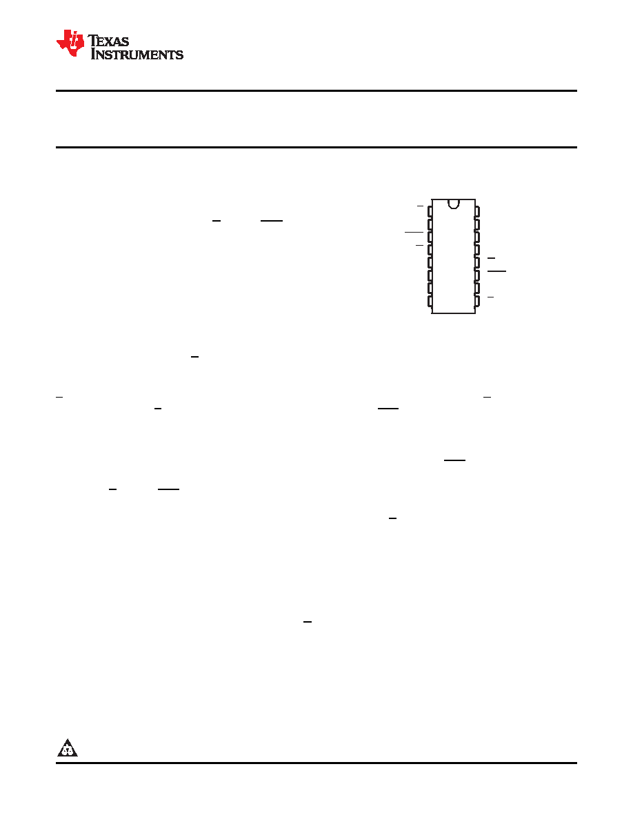
PW PACKAGE
(TOP VIEW)
1
2
3
4
5
6
7
8
16
15
14
13
12
11
10
9
1A
1B
1CLR
1Q
2Q
2Cext
2Rext/Cext
GND
VCC
1Rext/Cext
1Cext
1Q
2Q
2CLR
2B
2A
SCLS692A
– OCTOBER 2005 – REVISED APRIL 2008
DUAL MONOSTABLE MULTIVIBRATOR
WITH SCHMITT-TRIGGER INPUTS
Check for Samples: SN74LV221A-Q1
1
FEATURES
Qualified for Automotive Applications
2-V to 5.5-V VCC Operation
Supports Mixed-Mode Voltage Operation on
All Ports
Schmitt-Trigger Circuitry on A, B, and CLR
Inputs for Slow Transition Rates
Overriding Clear Terminates Output Pulse
Glitch-Free Power-Up Reset on Outputs
Ioff Supports Partial-Power-Down Mode
Operation
DESCRIPTION/ORDERING INFORMATION
The SN74LV221A is a dual multivibrator designed for 2-V to 5.5-V VCC operation. Each multivibrator has a
negative-transition-triggered (A) input and a positive-transition-triggered (B) input, either of which can be used as
an inhibit input.
This edge-triggered multivibrator features output pulse-duration control by three methods. In the first method, the
A input is low and the B input goes high. In the second method, the B input is high and the A input goes low. In
the third method, the A input is low, the B input is high, and the clear (CLR) input goes high.
The output pulse duration is programmable by selecting external resistance and capacitance values. The
external timing capacitor must be connected between Cext and Rext/Cext(positive) and an external resistor
connected between Rext/Cext and VCC. To obtain variable pulse durations, connect an external variable resistor
between Rext/Cext and VCC. The output pulse duration also can be reduced by taking CLR low.
Pulse triggering occurs at a particular voltage level and is not related directly to the transition time of the input
pulse. The A, B, and CLR inputs have Schmitt triggers with sufficient hysteresis to handle slow input transition
rates with jitter-free triggering at the outputs.
Once triggered, the outputs are independent of further transitions of the A and B inputs and are a function of the
timing components, or the output pulses can be terminated by the overriding clear. Input pulses can be of any
duration relative to the output pulse. Output pulse duration can be varied by choosing the appropriate timing
components. Output rise and fall times are TTL compatible and independent of pulse duration. Typical triggering
and clearing sequences are illustrated in the input/output timing diagram.
The variance in output pulse duration from device to device typically is less than
±0.5% for given external timing
components. An example of this distribution for the SN74LV221A-Q1 is shown in Figure 8. Variations in output
pulse duration versus supply voltage and temperature are shown in Figure 5.
During power up, Q outputs are in the low state, and Q outputs are in the high state. The outputs are glitch free,
without applying a reset pulse.
This device is fully specified for partial-power-down applications using Ioff. The Ioff circuitry disables the outputs,
preventing damaging current backflow through the devices when they are powered down.
1
Please be aware that an important notice concerning availability, standard warranty, and use in critical applications of Texas
Instruments semiconductor products and disclaimers thereto appears at the end of this data sheet.
UNLESS
OTHERWISE
NOTED
this
document
contains
Copyright
2005–2008, Texas Instruments Incorporated
PRODUCTION DATA information current as of publication date.
Products conform to specifications per the terms of Texas
Instruments standard warranty. Production processing does not
necessarily include testing of all parameters.
相關PDF資料 |
PDF描述 |
|---|---|
| SN74LV240ADGVRG4 | LV/LV-A/LVX/H SERIES, DUAL 4-BIT DRIVER, INVERTED OUTPUT, PDSO20 |
| SN74LV244AD | LV/LV-A/LVX/H SERIES, DUAL 4-BIT DRIVER, TRUE OUTPUT, PDSO20 |
| SN74LV244APWT | LV/LV-A/LVX/H SERIES, DUAL 4-BIT DRIVER, TRUE OUTPUT, PDSO20 |
| SN74LV244ADGVR | LV/LV-A/LVX/H SERIES, DUAL 4-BIT DRIVER, TRUE OUTPUT, PDSO20 |
| SN74LV244ADW | LV/LV-A/LVX/H SERIES, DUAL 4-BIT DRIVER, TRUE OUTPUT, PDSO20 |
相關代理商/技術參數 |
參數描述 |
|---|---|
| SN74LV221AQPWRQ1 | 功能描述:單穩態多諧振蕩器 Auto Cat Dual Mono Multivibrators RoHS:否 制造商:Texas Instruments 每芯片元件:1 邏輯系列:LVC 邏輯類型:Monostable Multivibrator 封裝 / 箱體:SSOP-8 傳播延遲時間:18.6 ns 高電平輸出電流:- 32 mA 低電平輸出電流:32 mA 電源電壓-最大:5.5 V 電源電壓-最小:1.65 V 最大功率耗散: 最大工作溫度:+ 85 C 最小工作溫度:- 40 C 封裝:Reel |
| SN74LV240ADBR | 功能描述:緩沖器和線路驅動器 Tri-State Octal RoHS:否 制造商:Micrel 輸入線路數量:1 輸出線路數量:2 極性:Non-Inverting 電源電壓-最大:+/- 5.5 V 電源電壓-最小:+/- 2.37 V 最大工作溫度:+ 85 C 安裝風格:SMD/SMT 封裝 / 箱體:MSOP-8 封裝:Reel |
| SN74LV240ADBRE4 | 功能描述:緩沖器和線路驅動器 Octal Buffer/Driver With 3-State Outputs RoHS:否 制造商:Micrel 輸入線路數量:1 輸出線路數量:2 極性:Non-Inverting 電源電壓-最大:+/- 5.5 V 電源電壓-最小:+/- 2.37 V 最大工作溫度:+ 85 C 安裝風格:SMD/SMT 封裝 / 箱體:MSOP-8 封裝:Reel |
| SN74LV240ADBRG4 | 功能描述:緩沖器和線路驅動器 Octal Buffers Driver RoHS:否 制造商:Micrel 輸入線路數量:1 輸出線路數量:2 極性:Non-Inverting 電源電壓-最大:+/- 5.5 V 電源電壓-最小:+/- 2.37 V 最大工作溫度:+ 85 C 安裝風格:SMD/SMT 封裝 / 箱體:MSOP-8 封裝:Reel |
| SN74LV240ADGVR | 功能描述:緩沖器和線路驅動器 Tri-State Octal RoHS:否 制造商:Micrel 輸入線路數量:1 輸出線路數量:2 極性:Non-Inverting 電源電壓-最大:+/- 5.5 V 電源電壓-最小:+/- 2.37 V 最大工作溫度:+ 85 C 安裝風格:SMD/SMT 封裝 / 箱體:MSOP-8 封裝:Reel |
發布緊急采購,3分鐘左右您將得到回復。