- 您現在的位置:買賣IC網 > PDF目錄98125 > SN74LVC373APWE4 (TEXAS INSTRUMENTS INC) LVC/LCX/Z SERIES, 8-BIT DRIVER, TRUE OUTPUT, PDSO20 PDF資料下載
參數資料
| 型號: | SN74LVC373APWE4 |
| 廠商: | TEXAS INSTRUMENTS INC |
| 元件分類: | 總線收發器 |
| 英文描述: | LVC/LCX/Z SERIES, 8-BIT DRIVER, TRUE OUTPUT, PDSO20 |
| 封裝: | GREEN, PLASTIC, TSSOP-20 |
| 文件頁數: | 1/29頁 |
| 文件大小: | 1122K |
| 代理商: | SN74LVC373APWE4 |
當前第1頁第2頁第3頁第4頁第5頁第6頁第7頁第8頁第9頁第10頁第11頁第12頁第13頁第14頁第15頁第16頁第17頁第18頁第19頁第20頁第21頁第22頁第23頁第24頁第25頁第26頁第27頁第28頁第29頁
www.ti.com
FEATURES
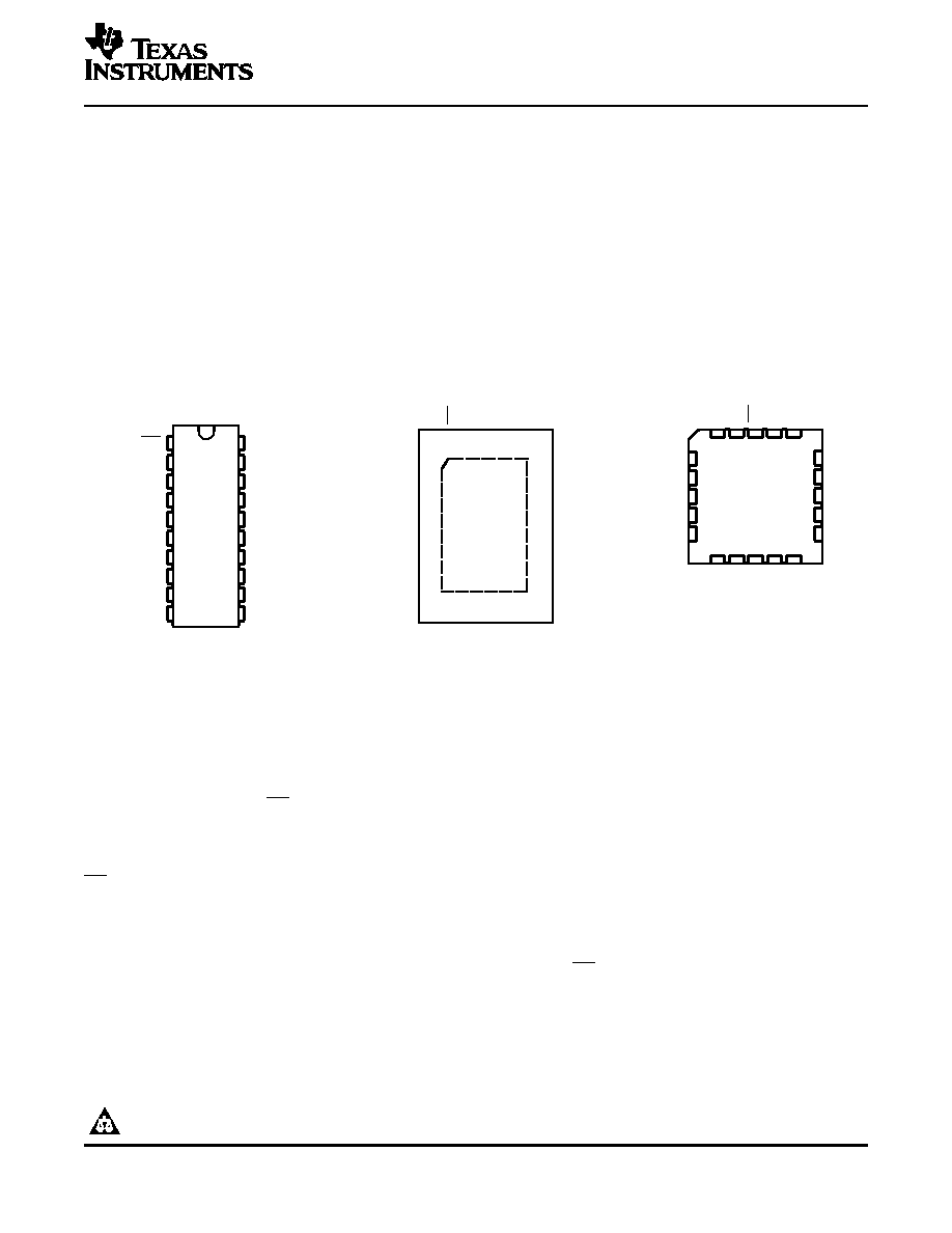
SN74LVC373A . . . RGY PACKAGE
(TOP VIEW)
1
20
10
11
2
3
4
5
6
7
8
9
19
18
17
16
15
14
13
12
8Q
8D
7D
7Q
6Q
6D
5D
5Q
1Q
1D
2D
2Q
3Q
3D
4D
4Q
LE
V
GND
CC
1
2
3
4
5
6
7
8
9
10
20
19
18
17
16
15
14
13
12
11
OE
1Q
1D
2D
2Q
3Q
3D
4D
4Q
GND
VCC
8Q
8D
7D
7Q
6Q
6D
5D
5Q
LE
SN54LVC373A . . . J OR W PACKAGE
SN74LVC373A . . . DB, DGV, DW, N,
NS, OR PW PACKAGE
(TOP VIEW)
SN54LVC373A . . . FK PACKAGE
(TOP VIEW)
3
2
1 20 19
9 10 11 12 13
4
5
6
7
8
18
17
16
15
14
2D
2Q
3Q
3D
4D
1D
1Q
OE
5Q
5D
8Q
4Q
GND
LE
V
CC
8D
7D
7Q
6Q
6D
OE
DESCRIPTION/ORDERING INFORMATION
SN54LVC373A, SN74LVC373A
OCTAL TRANSPARENT D-TYPE LATCHES
WITH 3-STATE OUTPUTS
SCAS295S – JANUARY 1993 – REVISED MAY 2005
Ioff Supports Partial-Power-Down Mode
Operation
Operate From 1.65 V to 3.6 V
Latch-Up Performance Exceeds 250 mA Per
Inputs Accept Voltages to 5.5 V
JESD 17
Max tpd of 6.8 ns at 3.3 V
ESD Protection Exceeds JESD 22
Typical VOLP (Output Ground Bounce) < 0.8 V
– 2000-V Human-Body Model (A114-A)
at VCC = 3.3 V, TA = 25°C
– 200-V Machine Model (A115-A)
Typical VOHV (Output VOH Undershoot) > 2 V at
VCC = 3.3 V, TA = 25°C
– 1000-V Charged-Device Model (C101)
ABC
Support Mixed-Mode Signal Operation on All
Ports (5-V Input/Output Voltage With
3.3-V VCC)
The SN54LVC373A octal transparent D-type latch is designed for 2.7-V to 3.6-V VCC operation, and the
SN74LVC373A octal transparent D-type latch is designed for 1.65-V to 3.6-V VCC operation.
While the latch-enable (LE) input is high, the Q outputs follow the data (D) inputs. When LE is taken low, the Q
outputs are latched at the logic levels set up at the D inputs.
A buffered output-enable (OE) input can be used to place the eight outputs in either a normal logic state (high or
low logic levels) or the high-impedance state. In the high-impedance state, the outputs neither load nor drive the
bus lines significantly. The high-impedance state and increased drive provide the capability to drive bus lines
without interface or pullup components.
OE does not affect the internal operations of the latches. Old data can be retained or new data can be entered
while the outputs are in the high-impedance state.
These devices are fully specified for partial-power-down applications using Ioff. The Ioff circuitry disables the
outputs, preventing damaging current backflow through the devices when they are powered down.
To ensure the high-impedance state during power up or power down, OE should be tied to VCC through a pullup
resistor; the minimum value of the resistor is determined by the current-sinking capability of the driver.
Inputs can be driven from either 3.3-V or 5-V devices. This feature allows the use of these devices as translators
in a mixed 3.3-V/5-V system environment.
Please be aware that an important notice concerning availability, standard warranty, and use in critical applications of Texas
Instruments semiconductor products and disclaimers thereto appears at the end of this data sheet.
PRODUCTION DATA information is current as of publication date.
Copyright 1993–2005, Texas Instruments Incorporated
Products conform to specifications per the terms of the Texas
On products compliant to MIL-PRF-38535, all parameters are
Instruments standard warranty. Production processing does not
tested unless otherwise noted. On all other products, production
necessarily include testing of all parameters.
processing does not necessarily include testing of all parameters.
相關PDF資料 |
PDF描述 |
|---|---|
| SN74LVC3G04YEPR | LVC/LCX/Z SERIES, TRIPLE 1-INPUT INVERT GATE, BGA8 |
| SN74LVC3G04YEAR | LVC/LCX/Z SERIES, TRIPLE 1-INPUT INVERT GATE, BGA8 |
| SN74LVC3G06DCURG4 | LVC/LCX/Z SERIES, TRIPLE 1-INPUT INVERT GATE, PDSO8 |
| SN74LVC3G06DCUT | LVC/LCX/Z SERIES, TRIPLE 1-INPUT INVERT GATE, PDSO8 |
| SN74LVC3G06DCUR | LVC/LCX/Z SERIES, TRIPLE 1-INPUT INVERT GATE, PDSO8 |
相關代理商/技術參數 |
參數描述 |
|---|---|
| SN74LVC373APWG4 | 功能描述:閉鎖 Octal Transparent RoHS:否 制造商:Micrel 電路數量:1 邏輯類型:CMOS 邏輯系列:TTL 極性:Non-Inverting 輸出線路數量:9 高電平輸出電流: 低電平輸出電流: 傳播延遲時間: 電源電壓-最大:12 V 電源電壓-最小:5 V 最大工作溫度:+ 85 C 最小工作溫度:- 40 C 封裝 / 箱體:SOIC-16 封裝:Reel |
| SN74LVC373APWR | 功能描述:閉鎖 Tri-St Octal D-Type RoHS:否 制造商:Micrel 電路數量:1 邏輯類型:CMOS 邏輯系列:TTL 極性:Non-Inverting 輸出線路數量:9 高電平輸出電流: 低電平輸出電流: 傳播延遲時間: 電源電壓-最大:12 V 電源電壓-最小:5 V 最大工作溫度:+ 85 C 最小工作溫度:- 40 C 封裝 / 箱體:SOIC-16 封裝:Reel |
| SN74LVC373APWR | 制造商:Texas Instruments 功能描述:IC 74LVC SMD 74LVC373 TSSOP20 |
| SN74LVC373APWRE4 | 功能描述:閉鎖 Tri-St Octal D-Type RoHS:否 制造商:Micrel 電路數量:1 邏輯類型:CMOS 邏輯系列:TTL 極性:Non-Inverting 輸出線路數量:9 高電平輸出電流: 低電平輸出電流: 傳播延遲時間: 電源電壓-最大:12 V 電源電壓-最小:5 V 最大工作溫度:+ 85 C 最小工作溫度:- 40 C 封裝 / 箱體:SOIC-16 封裝:Reel |
| SN74LVC373APWRG4 | 功能描述:閉鎖 Tri-St Octal D-Type RoHS:否 制造商:Micrel 電路數量:1 邏輯類型:CMOS 邏輯系列:TTL 極性:Non-Inverting 輸出線路數量:9 高電平輸出電流: 低電平輸出電流: 傳播延遲時間: 電源電壓-最大:12 V 電源電壓-最小:5 V 最大工作溫度:+ 85 C 最小工作溫度:- 40 C 封裝 / 箱體:SOIC-16 封裝:Reel |
發布緊急采購,3分鐘左右您將得到回復。