- 您現在的位置:買賣IC網 > PDF目錄98127 > SN74LVTH16835DLG4 (TEXAS INSTRUMENTS INC) LVT SERIES, 18-BIT DRIVER, TRUE OUTPUT, PDSO56 PDF資料下載
參數資料
| 型號: | SN74LVTH16835DLG4 |
| 廠商: | TEXAS INSTRUMENTS INC |
| 元件分類: | 總線收發器 |
| 英文描述: | LVT SERIES, 18-BIT DRIVER, TRUE OUTPUT, PDSO56 |
| 封裝: | GREEN, PLASTIC, SSOP-56 |
| 文件頁數: | 1/13頁 |
| 文件大小: | 359K |
| 代理商: | SN74LVTH16835DLG4 |
SN54LVTH16835, SN74LVTH16835
3.3-V ABT 18-BIT UNIVERSAL BUS DRIVERS
WITH 3-STATE OUTPUTS
SCBS713C – MARCH 1998 – REVISED APRIL 1999
1
POST OFFICE BOX 655303
DALLAS, TEXAS 75265
D Members of the Texas Instruments
Widebus
Family
D State-of-the-Art Advanced BiCMOS
Technology (ABT) Design for 3.3-V
Operation and Low Static-Power
Dissipation
D Support Mixed-Mode Signal Operation
(5-V Input and Output Voltages With
3.3-V VCC)
D Support Unregulated Battery Operation
Down to 2.7 V
D Typical VOLP (Output Ground Bounce)
< 0.8 V at VCC = 3.3 V, TA = 25°C
D Ioff and Power-Up 3-State Support Hot
Insertion
D Bus Hold on Data Inputs Eliminates the
Need for External Pullup/Pulldown
Resistors
D Distributed VCC and GND Pin Configuration
Minimizes High-Speed Switching Noise
D Flow-Through Architecture Optimizes PCB
Layout
D Latch-Up Performance Exceeds 500 mA Per
JESD 17
D ESD Protection Exceeds 2000 V Per
MIL-STD-883, Method 3015; Exceeds 200 V
Using Machine Model (C = 200 pF, R = 0)
D Package Options Include Plastic Shrink
Small-Outline (DL) and Thin Shrink
Small-Outline (DGG) Packages and 380-mil
Fine-Pitch Ceramic Flat (WD) Package
Using 25-mil Center-to-Center Spacings
description
The ’LVTH16835 devices are 18-bit universal bus drivers designed for low-voltage (3.3-V) VCC operation, but
with the capability to provide a TTL interface to a 5-V system environment.
Data flow from A to Y is controlled by the output-enable (OE) input. These devices operate in the transparent
mode when the latch-enable (LE) input is high. The A data is latched if the clock (CLK) input is held at a high
or low logic level. If LE is low, the A data is stored in the latch/flip-flop on the low-to-high transition of the clock.
When OE is high, the outputs are in the high-impedance state.
Active bus-hold circuitry is provided to hold unused or floating data inputs at a valid logic level.
When VCC is between 0 and 1.5 V, the devices are in the high-impedance state during power up or power down.
However, to ensure the high-impedance state above 1.5 V, OE should be tied to VCC through a pullup resistor;
the minimum value of the resistor is determined by the current-sinking capability of the driver.
Copyright
1999, Texas Instruments Incorporated
UNLESS OTHERWISE NOTED this document contains PRODUCTION
DATA information current as of publication date. Products conform to
specifications per the terms of Texas Instruments standard warranty.
Production processing does not necessarily include testing of all
parameters.
Widebus is a trademark of Texas Instruments Incorporated.
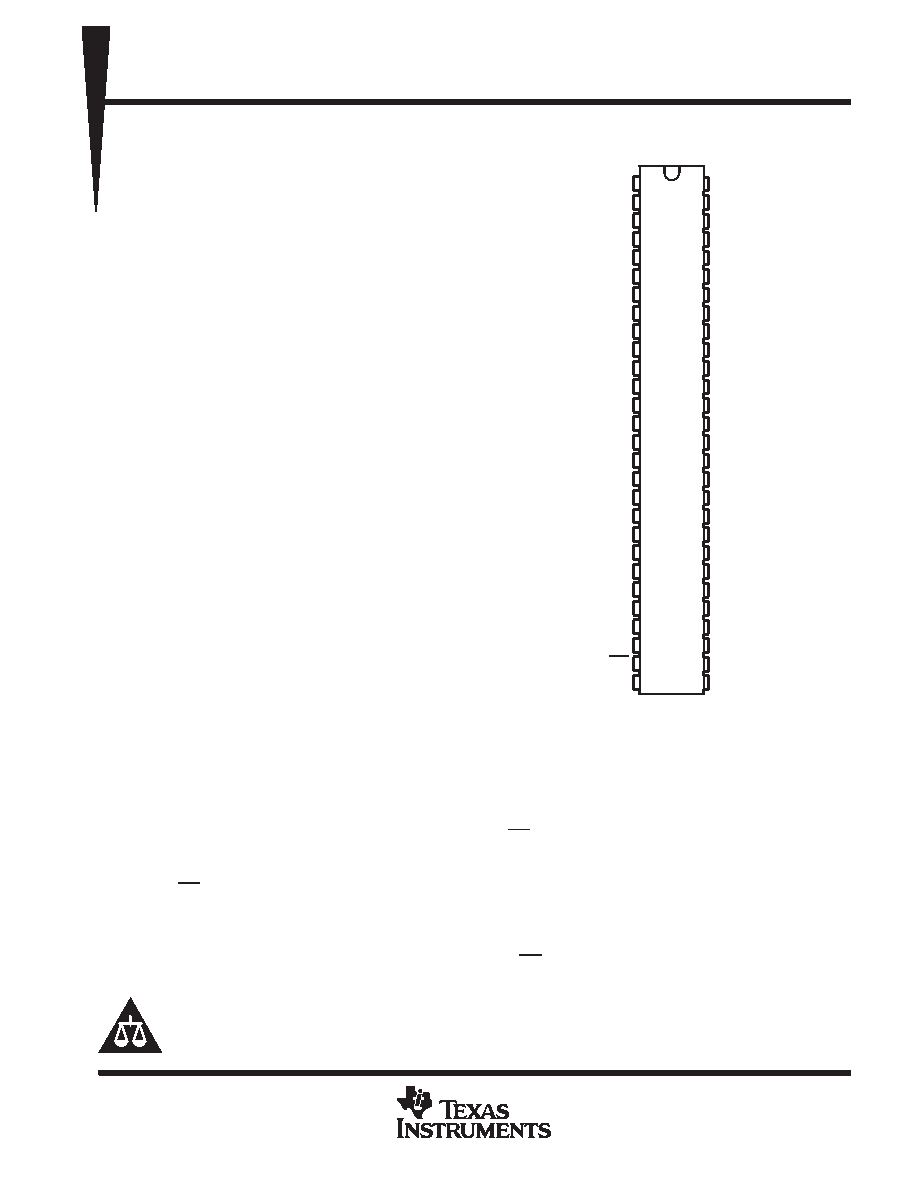
SN54LVTH16835 . . . WD PACKAGE
SN74LVTH16835 ... DGG OR DL PACKAGE
(TOP VIEW)
1
2
3
4
5
6
7
8
9
10
11
12
13
14
15
16
17
18
19
20
21
22
23
24
25
26
27
28
56
55
54
53
52
51
50
49
48
47
46
45
44
43
42
41
40
39
38
37
36
35
34
33
32
31
30
29
NC
Y1
GND
Y2
Y3
VCC
Y4
Y5
Y6
GND
Y7
Y8
Y9
Y10
Y11
Y12
GND
Y13
Y14
Y15
VCC
Y16
Y17
GND
Y18
OE
LE
GND
NC
A1
GND
A2
A3
VCC
A4
A5
A6
GND
A7
A8
A9
A10
A11
A12
GND
A13
A14
A15
VCC
A16
A17
GND
A18
CLK
GND
NC – No internal connection
Please be aware that an important notice concerning availability, standard warranty, and use in critical applications of
Texas Instruments semiconductor products and disclaimers thereto appears at the end of this data sheet.
相關PDF資料 |
PDF描述 |
|---|---|
| SN74LVTH16952DLR | LVT SERIES, DUAL 8-BIT REGISTERED TRANSCEIVER, TRUE OUTPUT, PDSO56 |
| SN74LVTH182514DGG | LVT SERIES, 20-BIT BOUNDARY SCAN REG TRANSCEIVER, TRUE OUTPUT, PDSO64 |
| SN74LVTH18514DGG | LVT SERIES, 20-BIT BOUNDARY SCAN REG TRANSCEIVER, TRUE OUTPUT, PDSO64 |
| SN74LVTH18640DL | LVT SERIES, DUAL 9-BIT BOUNDARY SCAN TRANSCEIVER, INVERTED OUTPUT, PDSO56 |
| SN74LVTH18640DGGR | LVT SERIES, DUAL 9-BIT BOUNDARY SCAN TRANSCEIVER, INVERTED OUTPUT, PDSO56 |
相關代理商/技術參數 |
參數描述 |
|---|---|
| SN74LVTH16835DLR | 功能描述:總線收發器 3.3V ABT 18-Bit Univ Bus Drvr W/3-St Otpt RoHS:否 制造商:Fairchild Semiconductor 邏輯類型:CMOS 邏輯系列:74VCX 每芯片的通道數量:16 輸入電平:CMOS 輸出電平:CMOS 輸出類型:3-State 高電平輸出電流:- 24 mA 低電平輸出電流:24 mA 傳播延遲時間:6.2 ns 電源電壓-最大:2.7 V, 3.6 V 電源電壓-最小:1.65 V, 2.3 V 最大工作溫度:+ 85 C 封裝 / 箱體:TSSOP-48 封裝:Reel |
| SN74LVTH16952DGGR | 功能描述:總線收發器 16bit ABT RoHS:否 制造商:Fairchild Semiconductor 邏輯類型:CMOS 邏輯系列:74VCX 每芯片的通道數量:16 輸入電平:CMOS 輸出電平:CMOS 輸出類型:3-State 高電平輸出電流:- 24 mA 低電平輸出電流:24 mA 傳播延遲時間:6.2 ns 電源電壓-最大:2.7 V, 3.6 V 電源電壓-最小:1.65 V, 2.3 V 最大工作溫度:+ 85 C 封裝 / 箱體:TSSOP-48 封裝:Reel |
| SN74LVTH16952DL | 功能描述:總線收發器 16bit ABT RoHS:否 制造商:Fairchild Semiconductor 邏輯類型:CMOS 邏輯系列:74VCX 每芯片的通道數量:16 輸入電平:CMOS 輸出電平:CMOS 輸出類型:3-State 高電平輸出電流:- 24 mA 低電平輸出電流:24 mA 傳播延遲時間:6.2 ns 電源電壓-最大:2.7 V, 3.6 V 電源電壓-最小:1.65 V, 2.3 V 最大工作溫度:+ 85 C 封裝 / 箱體:TSSOP-48 封裝:Reel |
| SN74LVTH16952DLG4 | 功能描述:總線收發器 10-Bit Buffer/Driver With 3-State Outputs RoHS:否 制造商:Fairchild Semiconductor 邏輯類型:CMOS 邏輯系列:74VCX 每芯片的通道數量:16 輸入電平:CMOS 輸出電平:CMOS 輸出類型:3-State 高電平輸出電流:- 24 mA 低電平輸出電流:24 mA 傳播延遲時間:6.2 ns 電源電壓-最大:2.7 V, 3.6 V 電源電壓-最小:1.65 V, 2.3 V 最大工作溫度:+ 85 C 封裝 / 箱體:TSSOP-48 封裝:Reel |
| SN74LVTH16952DLR | 功能描述:總線收發器 3.3 V ABT 16-Bit Reg Trncvr W/3-St Otpt RoHS:否 制造商:Fairchild Semiconductor 邏輯類型:CMOS 邏輯系列:74VCX 每芯片的通道數量:16 輸入電平:CMOS 輸出電平:CMOS 輸出類型:3-State 高電平輸出電流:- 24 mA 低電平輸出電流:24 mA 傳播延遲時間:6.2 ns 電源電壓-最大:2.7 V, 3.6 V 電源電壓-最小:1.65 V, 2.3 V 最大工作溫度:+ 85 C 封裝 / 箱體:TSSOP-48 封裝:Reel |
發布緊急采購,3分鐘左右您將得到回復。