- 您現(xiàn)在的位置:買賣IC網(wǎng) > PDF目錄98130 > SN74S374NSRG4 (TEXAS INSTRUMENTS INC) S SERIES, 8-BIT DRIVER, TRUE OUTPUT, PDSO20 PDF資料下載
參數(shù)資料
| 型號: | SN74S374NSRG4 |
| 廠商: | TEXAS INSTRUMENTS INC |
| 元件分類: | 總線收發(fā)器 |
| 英文描述: | S SERIES, 8-BIT DRIVER, TRUE OUTPUT, PDSO20 |
| 封裝: | GREEN, PLASTIC, SOP-20 |
| 文件頁數(shù): | 1/26頁 |
| 文件大小: | 793K |
| 代理商: | SN74S374NSRG4 |
當(dāng)前第1頁第2頁第3頁第4頁第5頁第6頁第7頁第8頁第9頁第10頁第11頁第12頁第13頁第14頁第15頁第16頁第17頁第18頁第19頁第20頁第21頁第22頁第23頁第24頁第25頁第26頁
SN54LS373, SN54LS374, SN54S373, SN54S374,
SN74LS373, SN74LS374, SN74S373, SN74S374
OCTAL D-TYPE TRANSPARENT LATCHES AND EDGE-TRIGGERED FLIP-FLOPS
SDLS165B – OCTOBER 1975 – REVISED AUGUST 2002
1
POST OFFICE BOX 655303
DALLAS, TEXAS 75265
D Choice of Eight Latches or Eight D-Type
Flip-Flops in a Single Package
D 3-State Bus-Driving Outputs
D Full Parallel Access for Loading
D Buffered Control Inputs
D Clock-Enable Input Has Hysteresis to
Improve Noise Rejection (’S373 and ’S374)
D P-N-P Inputs Reduce DC Loading on Data
Lines (’S373 and ’S374)
description
These 8-bit registers feature 3-state outputs
designed specifically for driving highly capacitive
or
relatively
low-impedance
loads.
The
high-impedance
3-state
and
increased
high-logic-level drive provide these registers with
the capability of being connected directly to and
driving the bus lines in a bus-organized system
without need for interface or pullup components.
These devices are particularly attractive for
implementing
buffer
registers,
I/O
ports,
bidirectional bus drivers, and working registers.
The eight latches of the ’LS373 and ’S373 are
transparent D-type latches, meaning that while
the enable (C or CLK) input is high, the Q outputs
follow the data (D) inputs. When C or CLK is taken
low, the output is latched at the level of the data
that was set up.
The eight flip-flops of the ’LS374 and ’S374 are
edge-triggered D-type flip-flops. On the positive
transition of the clock, the Q outputs are set to the
logic states that were set up at the D inputs.
Schmitt-trigger buffered inputs at the enable/clock lines of the ’S373 and ’S374 devices simplify system design
as ac and dc noise rejection is improved by typically 400 mV due to the input hysteresis. A buffered
output-control (OC) input can be used to place the eight outputs in either a normal logic state (high or low logic
levels) or the high-impedance state. In the high-impedance state, the outputs neither load nor drive the bus lines
significantly.
OC does not affect the internal operation of the latches or flip-flops. That is, the old data can be retained or new
data can be entered, even while the outputs are off.
Copyright
2002, Texas Instruments Incorporated
Please be aware that an important notice concerning availability, standard warranty, and use in critical applications of
Texas Instruments semiconductor products and disclaimers thereto appears at the end of this data sheet.
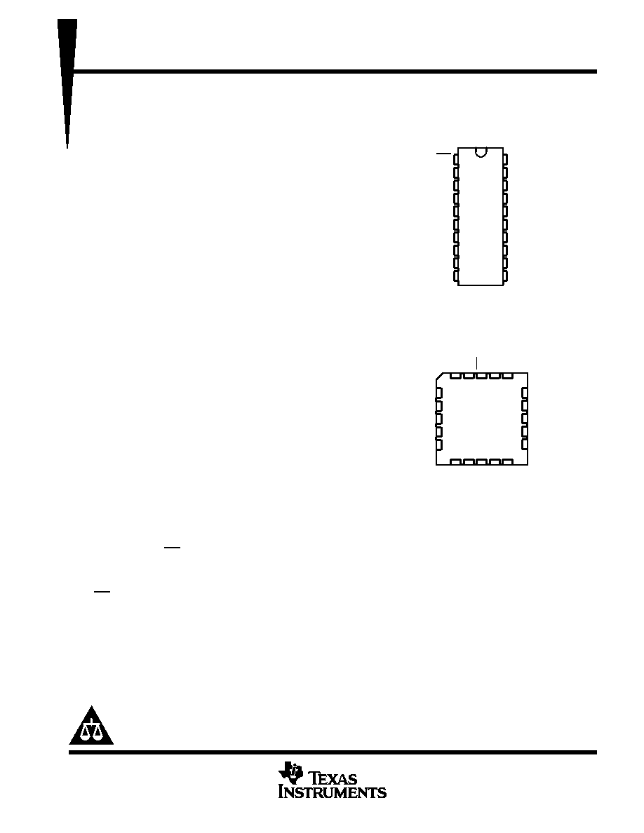
SN54LS373, SN54LS374, SN54S373,
SN54S374 . . . J OR W PACKAGE
SN74LS373, SN74S374 . . . DW, N, OR NS PACKAGE
SN74LS374 . . . DB, DW, N, OR NS PACKAGE
SN74S373 . . . DW OR N PACKAGE
(TOP VIEW)
32
1 20 19
910 11 12 13
4
5
6
7
8
18
17
16
15
14
8D
7D
7Q
6Q
6D
2D
2Q
3Q
3D
4D
SN54LS373, SN54LS374, SN54S373,
SN54S374 . . . FK PACKAGE
(TOP VIEW)
1D
1Q
OC
5Q
5D
8Q
4Q
GND
C
V
CC
1
2
3
4
5
6
7
8
9
10
20
19
18
17
16
15
14
13
12
11
OC
1Q
1D
2D
2Q
3Q
3D
4D
4Q
GND
VCC
8Q
8D
7D
7Q
6Q
6D
5D
5Q
C
C for ’LS373 and ’S373; CLK for ’LS374 and ’S374.
PRODUCTION DATA information is current as of publication date.
Products conform to specifications per the terms of Texas Instruments
standard warranty. Production processing does not necessarily include
testing of all parameters.
On products compliant to MIL-PRF-38535, all parameters are tested
unless otherwise noted. On all other products, production
processing does not necessarily include testing of all parameters.
相關(guān)PDF資料 |
PDF描述 |
|---|---|
| SN74S38DG4 | S SERIES, QUAD 2-INPUT NAND GATE, PDSO14 |
| SNJ54LS38FK | LS SERIES, QUAD 2-INPUT NAND GATE, CQCC20 |
| SN74S38DRG4 | S SERIES, QUAD 2-INPUT NAND GATE, PDSO14 |
| SN74LS38NSR | LS SERIES, QUAD 2-INPUT NAND GATE, PDSO14 |
| SN74S408D | DRAM CONTROLLER, MDIP48 |
相關(guān)代理商/技術(shù)參數(shù) |
參數(shù)描述 |
|---|---|
| SN74S374XC WAF | 制造商:Advanced Micro Devices 功能描述: |
| SN74S37D | 功能描述:邏輯門 Quad 2-input pos- NAND buffer RoHS:否 制造商:Texas Instruments 產(chǎn)品:OR 邏輯系列:LVC 柵極數(shù)量:2 線路數(shù)量(輸入/輸出):2 / 1 高電平輸出電流:- 16 mA 低電平輸出電流:16 mA 傳播延遲時間:3.8 ns 電源電壓-最大:5.5 V 電源電壓-最小:1.65 V 最大工作溫度:+ 125 C 安裝風(fēng)格:SMD/SMT 封裝 / 箱體:DCU-8 封裝:Reel |
| SN74S37DE4 | 功能描述:邏輯門 Quad 2-input pos- NAND buffer RoHS:否 制造商:Texas Instruments 產(chǎn)品:OR 邏輯系列:LVC 柵極數(shù)量:2 線路數(shù)量(輸入/輸出):2 / 1 高電平輸出電流:- 16 mA 低電平輸出電流:16 mA 傳播延遲時間:3.8 ns 電源電壓-最大:5.5 V 電源電壓-最小:1.65 V 最大工作溫度:+ 125 C 安裝風(fēng)格:SMD/SMT 封裝 / 箱體:DCU-8 封裝:Reel |
| SN74S37DG4 | 功能描述:邏輯門 Quad 2 input pos NAND buffer RoHS:否 制造商:Texas Instruments 產(chǎn)品:OR 邏輯系列:LVC 柵極數(shù)量:2 線路數(shù)量(輸入/輸出):2 / 1 高電平輸出電流:- 16 mA 低電平輸出電流:16 mA 傳播延遲時間:3.8 ns 電源電壓-最大:5.5 V 電源電壓-最小:1.65 V 最大工作溫度:+ 125 C 安裝風(fēng)格:SMD/SMT 封裝 / 箱體:DCU-8 封裝:Reel |
| SN74S37DR | 功能描述:邏輯門 Quad 2-input pos- NAND buffer RoHS:否 制造商:Texas Instruments 產(chǎn)品:OR 邏輯系列:LVC 柵極數(shù)量:2 線路數(shù)量(輸入/輸出):2 / 1 高電平輸出電流:- 16 mA 低電平輸出電流:16 mA 傳播延遲時間:3.8 ns 電源電壓-最大:5.5 V 電源電壓-最小:1.65 V 最大工作溫度:+ 125 C 安裝風(fēng)格:SMD/SMT 封裝 / 箱體:DCU-8 封裝:Reel |
發(fā)布緊急采購,3分鐘左右您將得到回復(fù)。