- 您現在的位置:買賣IC網 > PDF目錄376417 > SNJ54AHC05W (Texas Instruments, Inc.) HEX INVERTERS WITH OPEN-DRAIN OUTPUTS PDF資料下載
參數資料
| 型號: | SNJ54AHC05W |
| 廠商: | Texas Instruments, Inc. |
| 英文描述: | HEX INVERTERS WITH OPEN-DRAIN OUTPUTS |
| 中文描述: | 十六進制逆變器為開漏輸出 |
| 文件頁數: | 1/13頁 |
| 文件大小: | 333K |
| 代理商: | SNJ54AHC05W |
SN54AHC05, SN74AHC05
HEX INVERTERS
WITH OPEN-DRAIN OUTPUTS
SCLS357H – MAY 1997 – REVISED JULY 2003
1
POST OFFICE BOX 655303
DALLAS, TEXAS 75265
Operating Range 2-V to 5.5-V V
CC
Latch-Up Performance Exceeds 250 mA Per
JESD 17
ESD Protection Exceeds JESD 22
– 2000-V Human-Body Model (A114-A)
– 200-V Machine Model (A115-A)
– 1000-V Charged-Device Model (C101)
description/ordering information
The ’AHC05 devices contain six independent
inverters. These devices perform the Boolean
function Y = A.
The open-drain outputs require pullup resistors to
perform correctly. They can be connected to other
open-drain outputs to implement active-low
wired-OR or active-high wired-AND functions.
ORDERING INFORMATION
TA
PACKAGE
ORDERABLE
PART NUMBER
TOP-SIDE
MARKING
PDIP – N
Tube
SN74AHC05N
SN74AHC05N
SOIC – D
Tube
SN74AHC05D
AHC05
Tape and reel
SN74AHC05DR
–40
°
C to 85
°
C
SSOP – DB
Tape and reel
SN74AHC05DBR
HA05
TSSOP – PW
Tube
SN74AHC05PW
HA05
Tape and reel
SN74AHC05PWR
TVSOP – DGV
Tape and reel
SN74AHC05DGVR
HA05
CDIP – J
Tube
SNJ54AHC05J
SNJ54AHC05J
–55
°
C to 125
°
C
CFP – W
Tube
SNJ54AHC05W
SNJ54AHC05W
LCCC – FK
Tube
SNJ54AHC05FK
SNJ54AHC05FK
Package drawings, standard packing quantities, thermal data, symbolization, and PCB design guidelines
are available at www.ti.com/sc/package.
Copyright
2003, Texas Instruments Incorporated
UNLESS OTHERWISE NOTED this document contains PRODUCTION
specifications per the terms of Texas Instruments standard warranty.
parameters.
Please be aware that an important notice concerning availability, standard warranty, and use in critical applications of
Texas Instruments semiconductor products and disclaimers thereto appears at the end of this data sheet.
1
2
3
4
5
6
7
14
13
12
11
10
9
8
1A
1Y
2A
2Y
3A
3Y
GND
V
CC
6A
6Y
5A
5Y
4A
4Y
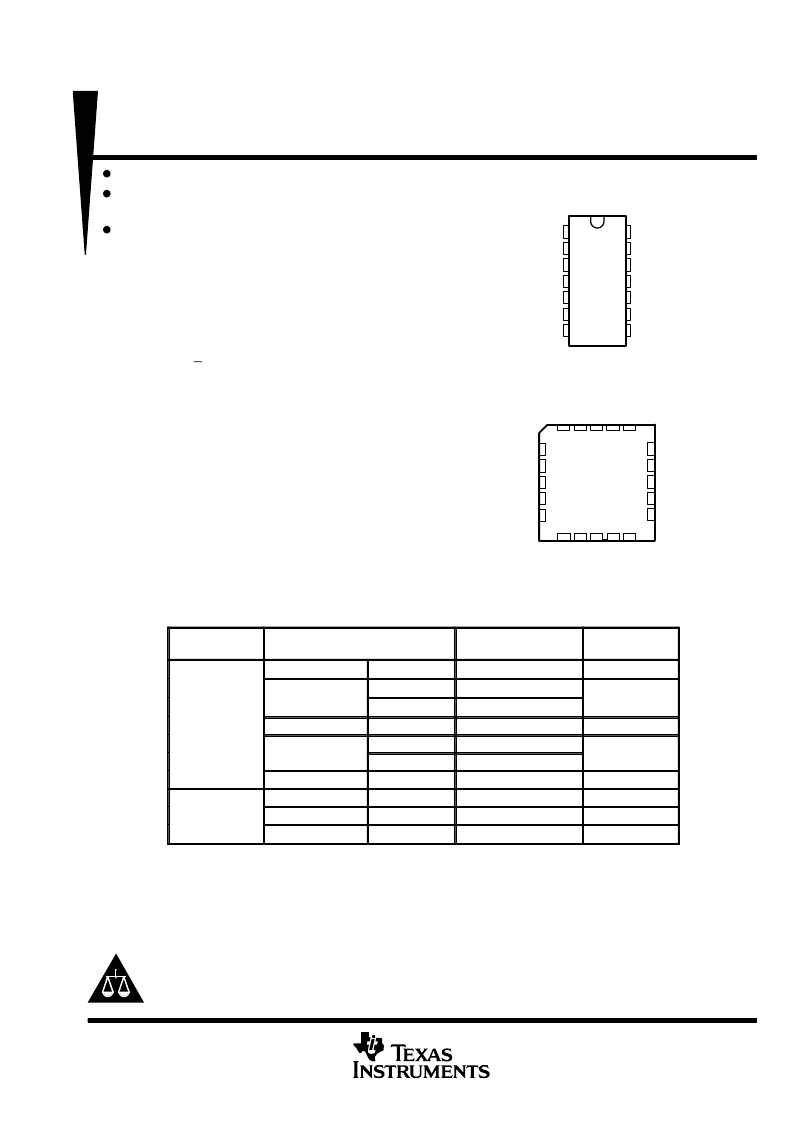
SN54AHC05 . . . J OR W PACKAGE
SN74AHC05 . . . D, DB, DGV, N, OR PW PACKAGE
(TOP VIEW)
3
2 1 20 19
9 10 11 12 13
4
5
6
7
8
18
17
16
15
14
6Y
NC
5A
NC
5Y
2A
NC
2Y
NC
3A
1
1
N
4
4
V
6
3
G
N
SN54AHC05 . . . FK PACKAGE
(TOP VIEW)
NC – No internal connection
相關PDF資料 |
PDF描述 |
|---|---|
| SNJ54AHCT594FK | 8-BIT SHIFT REGISTERS WITH OUTPUT REGISTERS |
| SNJ54AHCT594J | 8-BIT SHIFT REGISTERS WITH OUTPUT REGISTERS |
| SNJ54AHCT594W | 8-BIT SHIFT REGISTERS WITH OUTPUT REGISTERS |
| SNJ54LV123AFK | DUAL RETRIGGERABLE MONOSTABLE MULTIVIBRATORS WITH SCHMITT-TRIGGER INPUTS |
| SNJ54LV123AJ | DUAL RETRIGGERABLE MONOSTABLE MULTIVIBRATORS WITH SCHMITT-TRIGGER INPUTS |
相關代理商/技術參數 |
參數描述 |
|---|---|
| SNJ54AHC08FK | 制造商:Texas Instruments 功能描述:AND Gate 4-Element 2-IN CMOS 20-Pin LCCC Tube 制造商:Rochester Electronics LLC 功能描述:- Bulk |
| SNJ54AHC08J | 制造商:Texas Instruments 功能描述:AND Gate 4-Element 2-IN CMOS 14-Pin CDIP Tube |
| SNJ54AHC08W | 制造商:TI 制造商全稱:Texas Instruments 功能描述:HEX SCHMITT-TRIGGER INVERTERS |
| SNJ54AHC123AFK | 制造商:Texas Instruments 功能描述: |
| SNJ54AHC123AJ | 制造商:Texas Instruments 功能描述: |
發布緊急采購,3分鐘左右您將得到回復。