欧美成人免费电影,国产欧美一区二区三区精品酒店,精品国产a毛片,色网在线免费观看
參數資料
| 型號: | SY10EP01VKC |
| 廠商: | Micrel Inc |
| 文件頁數: | 5/6頁 |
| 文件大小: | 0K |
| 描述: | IC GATE OR/NOR 3.3V/5V 4IN 8MSOP |
| 標準包裝: | 100 |
| 系列: | 10EP |
| 邏輯類型: | 或非門/或門 |
| 電路數: | 1 |
| 輸入數: | 4 |
| 施密特觸發器輸入: | 無 |
| 輸出類型: | 差分 |
| 電源電壓: | 3 V ~ 5.5 V |
| 工作溫度: | -40°C ~ 85°C |
| 安裝類型: | 表面貼裝 |
| 封裝/外殼: | 8-TSSOP,8-MSOP(0.118",3.00mm 寬) |
| 供應商設備封裝: | 8-MSOP |
| 包裝: | 管件 |
IDT / ICS 3.3V, 2.5V LVPECL TRANSLATOR
5
ICS8532AMI REV A NOVEMBER 13, 2006
ICS85320I
LVCMOS/LVTTL-TO-DIFFERENTIAL 3.3V, 2.5V LVPECL TRANSLATOR
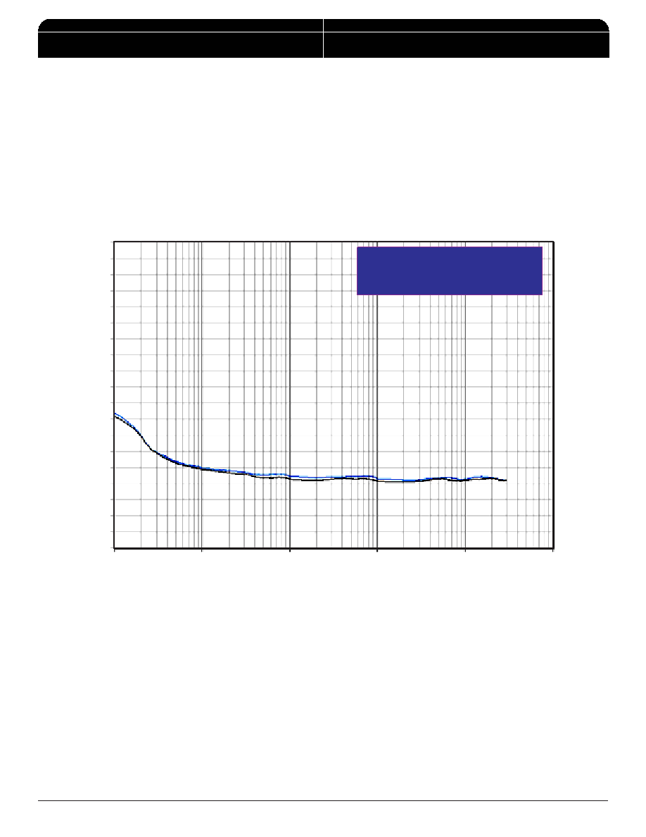
ADDITIVE PHASE JITTER
Input/Output Additive Phase Jitter
@ 156.25MHz (12KHz to 20MHz)
= 0.05ps typical
0
-10
-20
-30
-40
-50
-60
-70
-80
-90
-100
-110
-120
-130
-140
-150
-160
-170
-180
-190
1k
10k
100k
1M
10M
100M
The spectral purity in a band at a specific offset from the
fundamental compared to the power of the fundamental is called
the
dBc Phase Noise. This value is normally expressed using a
Phase noise plot and is most often the specified plot in many
applications. Phase noise is defined as the ratio of the noise power
present in a 1Hz band at a specified offset from the fundamental
frequency to the power value of the fundamental. This ratio is
expressed in decibels (dBm) or a ratio of the power in the 1Hz
As with most timing specifications, phase noise measurements
have issues. The primary issue relates to the limitations of the
equipment. Often the noise floor of the equipment is higher than
the noise floor of the device. This is illustrated above. The device
band to the power in the fundamental. When the required offset
is specified, the phase noise is called a
dBc value, which simply
means dBm at a specified offset from the fundamental. By
investigating jitter in the frequency domain, we get a better
understanding of its effects on the desired application over the
entire time record of the signal. It is mathematically possible to
calculate an expected bit error rate given a phase noise plot.
meets the noise floor of what is shown, but can actually be lower.
The phase noise is dependant on the input source and
measurement equipment.
OFFSET FROM CARRIER FREQUENCY (HZ)
SSB
P
HASE
N
OISE
dB
c
/H
Z
相關PDF資料 |
PDF描述 |
|---|---|
| TXR40AB00-1205AI | ADPTR TINEL LOCK STR SHELL 13, C |
| SY10EP08VKC TR | IC GATE XOR/XNOR 3.3V/5V 8-MSOP |
| TXR40AB00-1207AI | ADPTR TINEL LOCK STR SHELL 13, C |
| TXR40AB90-1408AI | ADPTR TINEL LOCK ANG SHELL 15, D |
| TXR18AB00C1206AI | ADPTR TINEL LOCK STR SHELL 12 |
相關代理商/技術參數 |
參數描述 |
|---|---|
| SY10EP01VKC TR | 功能描述:IC GATE OR/NOR 3.3V/5V 4IN 8MSOP RoHS:否 類別:集成電路 (IC) >> 邏輯 - 柵極和逆變器 - 多功能,可配置 系列:10EP 產品變化通告:Product Obsolescence 05/Oct/2010 標準包裝:100 系列:- 邏輯類型:可配置多功能 電路數:2 輸入數:2 施密特觸發器輸入:無 輸出類型:差分 輸出電流高,低:- 電源電壓:2.375 V ~ 3.465 V 工作溫度:-40°C ~ 70°C 安裝類型:表面貼裝 封裝/外殼:16-LBGA,FCBGA 供應商設備封裝:16-FCBGA(4x4) 包裝:帶卷 (TR) |
| SY10EP01VKG | 功能描述:邏輯門 3.3V/5V 4-input OR/NOR (I Temp, Green) RoHS:否 制造商:Texas Instruments 產品:OR 邏輯系列:LVC 柵極數量:2 線路數量(輸入/輸出):2 / 1 高電平輸出電流:- 16 mA 低電平輸出電流:16 mA 傳播延遲時間:3.8 ns 電源電壓-最大:5.5 V 電源電壓-最小:1.65 V 最大工作溫度:+ 125 C 安裝風格:SMD/SMT 封裝 / 箱體:DCU-8 封裝:Reel |
| SY10EP01VKG TR | 功能描述:邏輯門 3.3V/5V 4-input OR/NOR (I Temp, Green) RoHS:否 制造商:Texas Instruments 產品:OR 邏輯系列:LVC 柵極數量:2 線路數量(輸入/輸出):2 / 1 高電平輸出電流:- 16 mA 低電平輸出電流:16 mA 傳播延遲時間:3.8 ns 電源電壓-最大:5.5 V 電源電壓-最小:1.65 V 最大工作溫度:+ 125 C 安裝風格:SMD/SMT 封裝 / 箱體:DCU-8 封裝:Reel |
| SY10EP01VKI | 功能描述:IC GATE OR/NOR 3.3V/5V 4IN 8MSOP RoHS:否 類別:集成電路 (IC) >> 邏輯 - 柵極和逆變器 - 多功能,可配置 系列:10EP 產品變化通告:Product Obsolescence 05/Oct/2010 標準包裝:100 系列:- 邏輯類型:可配置多功能 電路數:2 輸入數:2 施密特觸發器輸入:無 輸出類型:差分 輸出電流高,低:- 電源電壓:2.375 V ~ 3.465 V 工作溫度:-40°C ~ 70°C 安裝類型:表面貼裝 封裝/外殼:16-LBGA,FCBGA 供應商設備封裝:16-FCBGA(4x4) 包裝:帶卷 (TR) |
| SY10EP01VKI TR | 功能描述:IC GATE OR/NOR 3.3V/5V 4IN 8MSOP RoHS:否 類別:集成電路 (IC) >> 邏輯 - 柵極和逆變器 - 多功能,可配置 系列:10EP 產品變化通告:Product Obsolescence 05/Oct/2010 標準包裝:100 系列:- 邏輯類型:可配置多功能 電路數:2 輸入數:2 施密特觸發器輸入:無 輸出類型:差分 輸出電流高,低:- 電源電壓:2.375 V ~ 3.465 V 工作溫度:-40°C ~ 70°C 安裝類型:表面貼裝 封裝/外殼:16-LBGA,FCBGA 供應商設備封裝:16-FCBGA(4x4) 包裝:帶卷 (TR) |
發布緊急采購,3分鐘左右您將得到回復。