- 您現在的位置:買賣IC網 > PDF目錄358432 > TC96C555COA (TelCom Semiconductor, Inc.) 3A OUTPUT PROGRAMMABLE POWER OSCILLATOR PDF資料下載
參數資料
| 型號: | TC96C555COA |
| 廠商: | TelCom Semiconductor, Inc. |
| 英文描述: | 3A OUTPUT PROGRAMMABLE POWER OSCILLATOR |
| 中文描述: | 3A輸出可編程功耗振蕩器 |
| 文件頁數: | 1/9頁 |
| 文件大小: | 106K |
| 代理商: | TC96C555COA |
4-159
TELCOM SEMICONDUCTOR, INC.
7
6
5
4
3
1
2
8
TC96C55
4
3
2
VDD
1V
2V
VREF
1V
2V 3V
Q1
Q2
1
3V
3V
ISOURCE
+4V
Q3
ISINK
7
6
OUTPUT A
OUTPUT B
5
GND
VREF
VR1
VIN
VR2
8
3A OUTPUT PROGRAMMABLE POWER OSCILLATOR
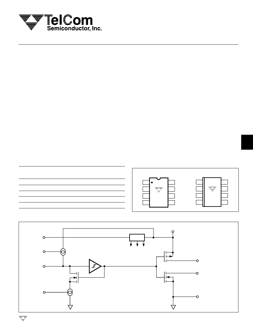
ORDERING INFORMATION
Operating
Temp Range
0
°
C to +70
°
C
0
°
C to +70
°
C
– 40
°
C to +85
°
C
– 40
°
C to +85
°
C
– 55
°
C to +125
°
C
Part No.
Package
TC96C555COA
TC96C555CPA
TC96C555EOA
TC96C555EPA
TC96C555MJA
8-Pin SOIC
8-Pin Plastic DIP
8-Pin SOIC
8-Pin Plastic DIP
8-Pin CerDIP
PIN CONFIGURATIONS
(DIP and SOIC)
1
8
2
7
3
6
4
5
VDD
VR1
VREF
VIN
VR2
OUT
OUT
GND
VR1
VREF
VIN
VR2
VDD
OUT
OUT
GND
1
8
2
7
3
6
4
5
TC96C555CPA
TC96C555EPA
TC96C555COA
TC96C555EOA
FUNCTIONAL BLOCK DIAGRAM
TC96C555-7 10/21/96
FEATURES
I
I
I
I
Controllable Duty Cycle
Wide Operating Range .............................5V to 18V
High Peak Output Current .................................. 3A
High Capacitive Load Drive
Capability .................................... 1800pF in 20nsec
Short Delay Time ............................. < 150nsec Typ
I
APPLICATIONS
I
I
I
I
I
Fixed Frequency Power Oscillator
Voltage Controlled Oscillator
Low Power Buck Regulator Supply
MOSFET Driver
Simple diode inverters and doublers
GENERAL DESCRIPTION
The TC96C555 Power Oscillator is an easily pro-
grammed IC that can be used in simple switch-mode power
supplies, diode doublers and inverters, and similar circuits
where high-current pulses are needed in an economical
form.
The TC96C555 uses TelCom Semiconductors' new
Tough CMOS process. The output drive capability is
similar to the TC4423/4/5 MOSFET Drivers, which can
switch in 25nsec into a capacitive load of 1,800pF. The
TC96C555 will not latch up under any conditions within their
power and voltage ratings. They can accept, without dam-
age, up to 1.5A of reverse current (of either polarity) being
forced back into the output. All terminals are also fully
protected against up to 4kV of electrostatic discharge. The
peak output is rated at 3A. Split outputs permits driving of an
external pair of MOSFETS, with controllable cross conduc-
tion between upper and lower devices.
相關PDF資料 |
PDF描述 |
|---|---|
| TC96C55 | 3A OUTPUT PROGRAMMABLE POWER OSCILLATOR |
| TC96C555CPA | 3A OUTPUT PROGRAMMABLE POWER OSCILLATOR |
| TC96C555EPA | 3A OUTPUT PROGRAMMABLE POWER OSCILLATOR |
| TC96C555MJA | 3A OUTPUT PROGRAMMABLE POWER OSCILLATOR |
| TCBZV55B2V4 | 2.4 V, 0.5 W, SILICON, UNIDIRECTIONAL VOLTAGE REGULATOR DIODE, DO-213AC |
相關代理商/技術參數 |
參數描述 |
|---|---|
| TC96C555CPA | 制造商:TELCOM 制造商全稱:TelCom Semiconductor, Inc 功能描述:3A OUTPUT PROGRAMMABLE POWER OSCILLATOR |
| TC96C555EOA | 制造商:TELCOM 制造商全稱:TelCom Semiconductor, Inc 功能描述:3A OUTPUT PROGRAMMABLE POWER OSCILLATOR |
| TC96C555EPA | 制造商:TELCOM 制造商全稱:TelCom Semiconductor, Inc 功能描述:3A OUTPUT PROGRAMMABLE POWER OSCILLATOR |
| TC96C555MJA | 制造商:TELCOM 制造商全稱:TelCom Semiconductor, Inc 功能描述:3A OUTPUT PROGRAMMABLE POWER OSCILLATOR |
| TC991 | 制造商:Brother 功能描述:TAPE SILVER 9MM |
發布緊急采購,3分鐘左右您將得到回復。