- 您現在的位置:買賣IC網 > PDF目錄98218 > THS1041IDW (TEXAS INSTRUMENTS INC) 1-CH 10-BIT PROPRIETARY METHOD ADC, PARALLEL ACCESS, PDSO28 PDF資料下載
參數資料
| 型號: | THS1041IDW |
| 廠商: | TEXAS INSTRUMENTS INC |
| 元件分類: | ADC |
| 英文描述: | 1-CH 10-BIT PROPRIETARY METHOD ADC, PARALLEL ACCESS, PDSO28 |
| 封裝: | GREEN, PLASTIC, SOIC-28 |
| 文件頁數: | 7/41頁 |
| 文件大小: | 810K |
| 代理商: | THS1041IDW |
第1頁第2頁第3頁第4頁第5頁第6頁當前第7頁第8頁第9頁第10頁第11頁第12頁第13頁第14頁第15頁第16頁第17頁第18頁第19頁第20頁第21頁第22頁第23頁第24頁第25頁第26頁第27頁第28頁第29頁第30頁第31頁第32頁第33頁第34頁第35頁第36頁第37頁第38頁第39頁第40頁第41頁
THS1041
SLAS289C OCTOBER 2001 REVISED OCTOBER 2004
15
www.ti.com
PRINCIPLES OF OPERATION
functional overview
Refer to functional block diagram. A single-ended, sample rate clock is required at pin CLK for device operation.
Analog inputs AIN+ and AIN are sampled on each rising edge of CLK in a switched capacitor sample and hold
unit, the output of which feeds a programmable gain amplifier (PGA) to the ADC core, where analog-to-digital
conversion is performed against the ADC reference voltages REFT and REFB.
Internal or external ADC reference voltage configurations are selected by connecting the MODE pin
appropriately. When MODE = AGND, the user must provide external sources at pins REFB and REFT. When
MODE = AVDD or MODE = AVDD/2, an internal ADC references generator (A2) is enabled, which drives the
REFT and REFB pins using the voltage at pin VREF as its input. The user can choose to drive VREF from the
internal bandgap reference, or they can disable A1 and provide their own reference voltage at pin VREF.
On the fourth rising CLK edge following the edge that sampled AIN+ and AIN, the conversion result is output
via data pins I/O0 to I/O9. The output buffers can be disabled by pulling pin OE high, allowing the user to place
device configuration data on the data pins, which are then latched into the internal control registers by strobing
the WR pin high then low. The internal registers control the data output format (unsigned or twos complement),
the PGA gain, device powerdown, the clamp functions, and the clamp DAC voltage.
The THS1041 offers a clamp circuit suitable for dc restoration of ac-coupled signals. The clamp voltage level
can be set using an external reference applied to the CLAMPIN pin, or it can be set to a reference level provided
by an on-chip 10-bit DAC. The CLAMPOUT pin must be connected externally to AIN+ or AIN in applications
requiring the clamp function.
The following sections explain further:
D How signals flow from AIN+ and AIN to the ADC core, and how the reference voltages at REFT and REFB
set the ADC input range and hence the input range at AIN+ and AIN
D How to set the ADC references REFT and REFB using external sources or the internal ADC reference buffer
(A2) to match the device input range to the input signal
D How to set the output of the internal bandgap reference (A1) if required
D How to use the clamp and device control registers
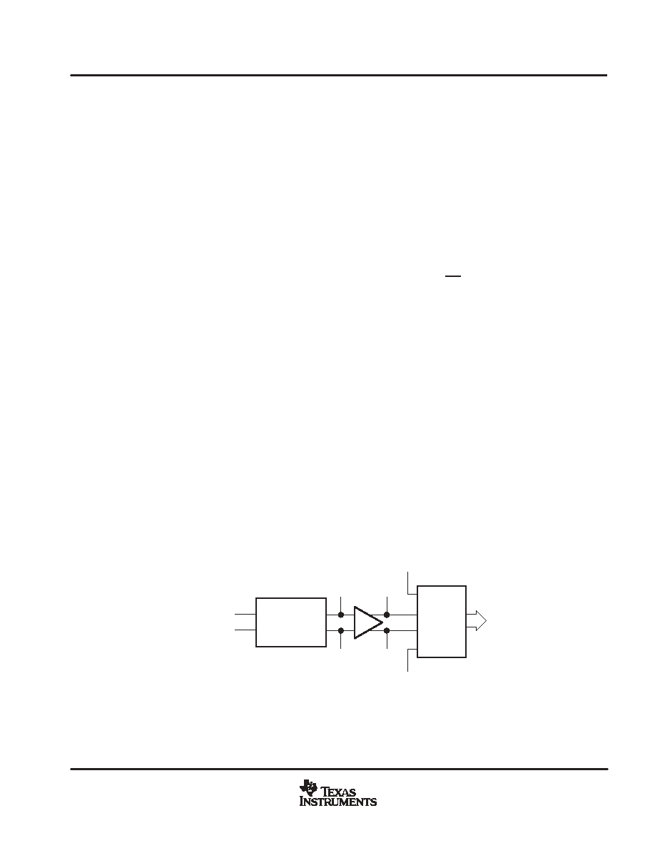
signal processing chain (sample and hold, PGA, ADC)
Figure 25 shows the signal flow through the sample and hold unit and the PGA to the ADC core.
Sample
and
Hold
X1
ADC
Core
VP+
VP
VQ+
VQ
REFT
REFB
AIN+
AIN
PGA
Figure 25. Analog Input Signal Flow
相關PDF資料 |
PDF描述 |
|---|---|
| THS1041IDWG4 | 1-CH 10-BIT PROPRIETARY METHOD ADC, PARALLEL ACCESS, PDSO28 |
| THS1041IPWR | 1-CH 10-BIT PROPRIETARY METHOD ADC, PARALLEL ACCESS, PDSO28 |
| THS1041IPWG4 | 1-CH 10-BIT PROPRIETARY METHOD ADC, PARALLEL ACCESS, PDSO28 |
| THS1050CPHP | 1-CH 10-BIT DELTA-SIGMA ADC, PARALLEL ACCESS, PQFP48 |
| THS1050IPHP | 1-CH 10-BIT DELTA-SIGMA ADC, PARALLEL ACCESS, PQFP48 |
相關代理商/技術參數 |
參數描述 |
|---|---|
| THS1041IDWG4 | 功能描述:模數轉換器 - ADC 10 Bit 40 MSPS Lo-Pwr RoHS:否 制造商:Texas Instruments 通道數量:2 結構:Sigma-Delta 轉換速率:125 SPs to 8 KSPs 分辨率:24 bit 輸入類型:Differential 信噪比:107 dB 接口類型:SPI 工作電源電壓:1.7 V to 3.6 V, 2.7 V to 5.25 V 最大工作溫度:+ 85 C 安裝風格:SMD/SMT 封裝 / 箱體:VQFN-32 |
| THS1041IDWR | 功能描述:模數轉換器 - ADC 10 Bit 40 MSPS Lo-Pwr RoHS:否 制造商:Texas Instruments 通道數量:2 結構:Sigma-Delta 轉換速率:125 SPs to 8 KSPs 分辨率:24 bit 輸入類型:Differential 信噪比:107 dB 接口類型:SPI 工作電源電壓:1.7 V to 3.6 V, 2.7 V to 5.25 V 最大工作溫度:+ 85 C 安裝風格:SMD/SMT 封裝 / 箱體:VQFN-32 |
| THS1041IDWRG4 | 功能描述:模數轉換器 - ADC 10 Bit 40 MSPS Lo-Pwr RoHS:否 制造商:Texas Instruments 通道數量:2 結構:Sigma-Delta 轉換速率:125 SPs to 8 KSPs 分辨率:24 bit 輸入類型:Differential 信噪比:107 dB 接口類型:SPI 工作電源電壓:1.7 V to 3.6 V, 2.7 V to 5.25 V 最大工作溫度:+ 85 C 安裝風格:SMD/SMT 封裝 / 箱體:VQFN-32 |
| THS1041IPW | 功能描述:模數轉換器 - ADC 10 Bit 40 MSPS Lo-Pwr RoHS:否 制造商:Texas Instruments 通道數量:2 結構:Sigma-Delta 轉換速率:125 SPs to 8 KSPs 分辨率:24 bit 輸入類型:Differential 信噪比:107 dB 接口類型:SPI 工作電源電壓:1.7 V to 3.6 V, 2.7 V to 5.25 V 最大工作溫度:+ 85 C 安裝風格:SMD/SMT 封裝 / 箱體:VQFN-32 |
| THS1041IPWG4 | 功能描述:模數轉換器 - ADC 10 Bit 40 MSPS Lo-Pwr RoHS:否 制造商:Texas Instruments 通道數量:2 結構:Sigma-Delta 轉換速率:125 SPs to 8 KSPs 分辨率:24 bit 輸入類型:Differential 信噪比:107 dB 接口類型:SPI 工作電源電壓:1.7 V to 3.6 V, 2.7 V to 5.25 V 最大工作溫度:+ 85 C 安裝風格:SMD/SMT 封裝 / 箱體:VQFN-32 |
發布緊急采購,3分鐘左右您將得到回復。