- 您現在的位置:買賣IC網 > PDF目錄98219 > THS1230CPW (TEXAS INSTRUMENTS INC) 1-CH 12-BIT PROPRIETARY METHOD ADC, PARALLEL ACCESS, PDSO28 PDF資料下載
參數資料
| 型號: | THS1230CPW |
| 廠商: | TEXAS INSTRUMENTS INC |
| 元件分類: | ADC |
| 英文描述: | 1-CH 12-BIT PROPRIETARY METHOD ADC, PARALLEL ACCESS, PDSO28 |
| 封裝: | GREEN, PLASTIC, TSSOP-28 |
| 文件頁數: | 3/25頁 |
| 文件大小: | 884K |
| 代理商: | THS1230CPW |
www.ti.com
140
120
100
80
60
40
20
0
0.88
1.76
2.64
3.53
4.41
5.29
6.17
7.05
7.93
8.81
9.69
10.6
1
1.5
12.3
13.2
14.1
15
Power
dBFS
f Frequency MHz
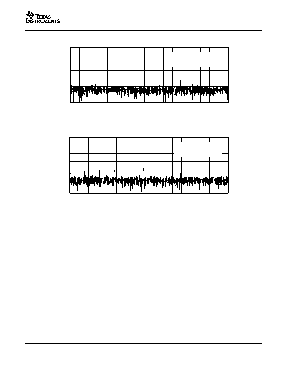
AVDD = DVDD = 3.3 V,
fs = 30 MSPS,
fi = 3.58 MHz, 1 dBFS,
Mode 1 Differential
140
120
100
80
60
40
20
0
0.88
1.76
2.64
3.53
4.41
5.29
6.17
7.05
7.93
8.81
9.69
10.6
1
1.5
12.3
13.2
14.1
15
AVDD = DVDD = 3.3 V,
fs = 30 MSPS,
fi = 3.58 MHz, 1 dBFS,
Mode 2 Differential
Power
dBFS
f Frequency MHz
PRINCIPLES OF OPERATION
Analog Input
THS1230
SLAS291B – OCTOBER 2000 – REVISED MARCH 2004
TYPICAL CHARACTERISTICS (continued)
FAST FOURIER TRANSFORM - MODE 1
Figure 12.
FAST FOURIER TRANSFORM - MODE 2
Figure 13.
The analog input AIN is sampled in the sample and hold unit, the output of which feeds the ADC CORE, where
the process of analog to digital conversion is performed against ADC reference voltages, VREFT and VREFB.
Connecting the EXTREF pin to one of two voltages, DGND or DVDD selects one of the two configurations of ADC
reference generation. The ADC reference voltages come from either the internal reference buffer or completely
external sources. Connect EXTREF to DGND for internal reference generation or to DVDD for external reference
generation.
CON0 and CON1 as described below, select the input configuration mode or place the device in powerdown.
The ADC core drives out through output buffers to the data pins D0 to D11. The output buffers can be disabled
by the OE pin.
A single, sample-rate clock (30 MHz maximum) is required at pin CLK. The analog input signal is sampled on the
rising edge of CLK, and corresponding data is output after the fifth following rising edge.
The THS1230 can operate in differential Mode 1 or differential Mode 2, controlled by the configuration pins
CON0 and CON1 as shown in Table 1. Mode 0 places the device in power-down state or standby for reduced
power consumption.
11
相關PDF資料 |
PDF描述 |
|---|---|
| THS1230CDW | 1-CH 12-BIT PROPRIETARY METHOD ADC, PARALLEL ACCESS, PDSO28 |
| THS1230IPWRG4 | 1-CH 12-BIT PROPRIETARY METHOD ADC, PARALLEL ACCESS, PDSO28 |
| THS1230CDWR | 1-CH 12-BIT PROPRIETARY METHOD ADC, PARALLEL ACCESS, PDSO28 |
| THS1230CPWG4 | 1-CH 12-BIT PROPRIETARY METHOD ADC, PARALLEL ACCESS, PDSO28 |
| THS1230CPWR | 1-CH 12-BIT PROPRIETARY METHOD ADC, PARALLEL ACCESS, PDSO28 |
相關代理商/技術參數 |
參數描述 |
|---|---|
| THS1230CPWG4 | 功能描述:模數轉換器 - ADC Low Power High-Speed ADC RoHS:否 制造商:Texas Instruments 通道數量:2 結構:Sigma-Delta 轉換速率:125 SPs to 8 KSPs 分辨率:24 bit 輸入類型:Differential 信噪比:107 dB 接口類型:SPI 工作電源電壓:1.7 V to 3.6 V, 2.7 V to 5.25 V 最大工作溫度:+ 85 C 安裝風格:SMD/SMT 封裝 / 箱體:VQFN-32 |
| THS1230CPWR | 功能描述:模數轉換器 - ADC Low Power High-Speed ADC RoHS:否 制造商:Texas Instruments 通道數量:2 結構:Sigma-Delta 轉換速率:125 SPs to 8 KSPs 分辨率:24 bit 輸入類型:Differential 信噪比:107 dB 接口類型:SPI 工作電源電壓:1.7 V to 3.6 V, 2.7 V to 5.25 V 最大工作溫度:+ 85 C 安裝風格:SMD/SMT 封裝 / 箱體:VQFN-32 |
| THS1230CPWRG4 | 功能描述:模數轉換器 - ADC Low Power High-Speed ADC RoHS:否 制造商:Texas Instruments 通道數量:2 結構:Sigma-Delta 轉換速率:125 SPs to 8 KSPs 分辨率:24 bit 輸入類型:Differential 信噪比:107 dB 接口類型:SPI 工作電源電壓:1.7 V to 3.6 V, 2.7 V to 5.25 V 最大工作溫度:+ 85 C 安裝風格:SMD/SMT 封裝 / 箱體:VQFN-32 |
| THS1230EVM | 功能描述:數據轉換 IC 開發工具 THS1230 Eval Mod RoHS:否 制造商:Texas Instruments 產品:Demonstration Kits 類型:ADC 工具用于評估:ADS130E08 接口類型:SPI 工作電源電壓:- 6 V to + 6 V |
| THS1230IDW | 功能描述:模數轉換器 - ADC Low Power High-Speed ADC RoHS:否 制造商:Texas Instruments 通道數量:2 結構:Sigma-Delta 轉換速率:125 SPs to 8 KSPs 分辨率:24 bit 輸入類型:Differential 信噪比:107 dB 接口類型:SPI 工作電源電壓:1.7 V to 3.6 V, 2.7 V to 5.25 V 最大工作溫度:+ 85 C 安裝風格:SMD/SMT 封裝 / 箱體:VQFN-32 |
發布緊急采購,3分鐘左右您將得到回復。