- 您現在的位置:買賣IC網 > PDF目錄383946 > THS3001D (Texas Instruments, Inc.) 420-MHz HIGH-SPEED CURRENT-FEEDBACK AMPLIFIERS PDF資料下載
參數資料
| 型號: | THS3001D |
| 廠商: | Texas Instruments, Inc. |
| 英文描述: | 420-MHz HIGH-SPEED CURRENT-FEEDBACK AMPLIFIERS |
| 中文描述: | 420 - MHz高速電流反饋放大器 |
| 文件頁數: | 1/32頁 |
| 文件大小: | 633K |
| 代理商: | THS3001D |
當前第1頁第2頁第3頁第4頁第5頁第6頁第7頁第8頁第9頁第10頁第11頁第12頁第13頁第14頁第15頁第16頁第17頁第18頁第19頁第20頁第21頁第22頁第23頁第24頁第25頁第26頁第27頁第28頁第29頁第30頁第31頁第32頁
THS3001, THS3002
420-MHz HIGH-SPEED CURRENT-FEEDBACK AMPLIFIERS
SLOS217A – JULY 1998 – REVISED JUNE 1999
1
POST OFFICE BOX 655303
DALLAS, TEXAS 75265
High Speed
– 420 MHz Bandwidth (G = 1, –3 dB)
– 6500 V/
μ
s Slew Rate
– 40-ns Settling Time (0.1%)
High Output Drive, I
O
= 100 mA
Excellent Video Performance
– 115 MHz Bandwidth (0.1 dB, G = 2)
– 0.01% Differential Gain
– 0.02
°
Differential Phase
Low 3-mV (max) Input Offset Voltage
Very Low Distortion
– THD = –96 dBc at f = 1 MHz
– THD = –80 dBc at f = 10 MHz
Wide Range of Power Supplies
– V
CC
=
±
4.5 V to
±
16 V
Evaluation Module Available
description
The THS300x is a high-speed current-feedback
operational amplifier, ideal for communication,
imaging, and high-quality video applications. This
device offers a very fast 6500-V/
μ
s slew rate, a
420-MHz bandwidth, and 40-ns settling time for
large-signal applications requiring excellent tran-
sient response. In addition, the THS300x
operates with a very low distortion of –96 dBc,
making it well suited for applications such as
wireless communication basestations or ultrafast
ADC or DAC buffers.
HIGH-SPEED AMPLIFIER FAMILY
DEVICE
ARCHITECTURE
SUPPLY
VOLTAGE
BW
(MHz)
SR
(V/
μ
s)
THD
f = 1 MHz
(dB)
ts
0.1%
(ns)
DIFF.
GAIN
DIFF.
PHASE
Vn
(nV/
√
Hz)
VFB
CFB
5 V
±
5 V
±
15 V
THS3001/02
420
6500
–96
40
0.01%
0.02
°
1.6
THS4001
270
400
–72
40
0.04%
0.15
°
0.01
°
0.03
°
0.02
°
12.5
THS4011/12
290
310
–80
37
0.006%
7.5
THS4031/32
100
100
–72
60
0.02%
1.6
THS4061/62
180
400
–72
40
0.02%
14.5
CAUTION: The THS300x provides ESD protection circuitry. However, permanent damage can still occur if this device is subjected
to high-energy electrostatic discharges. Proper ESD precautions are recommended to avoid any performance degradation or loss
of functionality.
Copyright
1999, Texas Instruments Incorporated
Please be aware that an important notice concerning availability, standard warranty, and use in critical applications of
Texas Instruments semiconductor products and disclaimers thereto appears at the end of this data sheet.
PRODUCTION DATA information is current as of publication date.
Products conform to specifications per the terms of Texas Instruments
standard warranty. Production processing does not necessarily include
testing of all parameters.
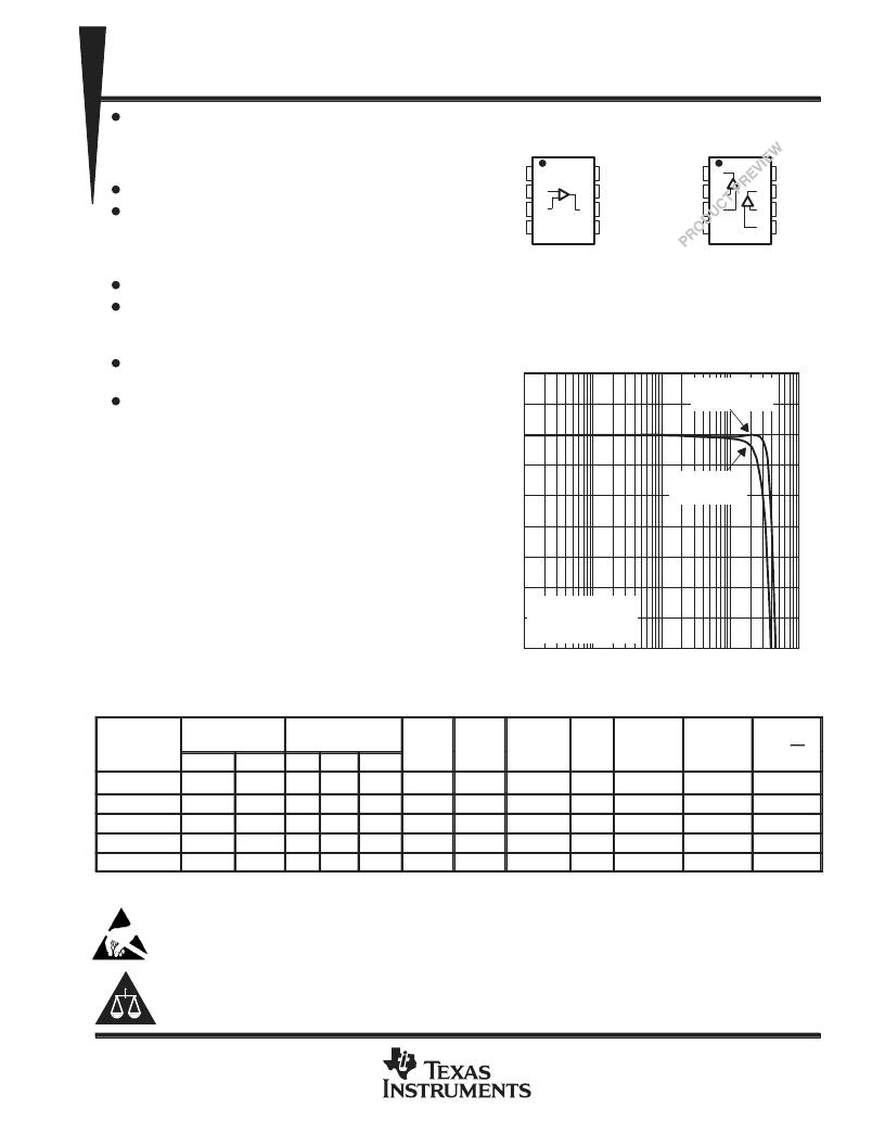
f – Frequency – Hz
OUTPUT AMPLITUDE
vs
FREQUENCY
5
3
1
–1
1M
100M
6
4
2
0
10M
1G
100k
7
8
O
G = 2
RL = 150
VI = 200 mV RMS
VCC =
±
5 V
RF = 750
VCC =
±
15 V
RF = 680
THS3002
D AND DGN PACKAGE
(TOP VIEW)
1
2
3
4
8
7
6
5
1OUT
1IN–
1IN+
–V
CC
V
CC+
2OUT
2IN–
2IN+
1
2
3
4
8
7
6
5
NULL
IN–
IN+
V
CC–
NULL
V
CC+
OUT
NC
THS3001
D AND DGN PACKAGE
(TOP VIEW)
NC – No internal connection
The THS3001 implemented in the DGN package is in the
product preview stage of development. Contact your local TI
sales office for availability.
相關PDF資料 |
PDF描述 |
|---|---|
| THS3002CDGN | 420-MHz HIGH-SPEED CURRENT-FEEDBACK AMPLIFIERS |
| THS3001DGN | 420-MHz HIGH-SPEED CURRENT-FEEDBACK AMPLIFIERS |
| THS3001EVM | 420-MHz HIGH-SPEED CURRENT-FEEDBACK AMPLIFIERS |
| THS3002 | 420-MHz HIGH-SPEED CURRENT-FEEDBACK AMPLIFIERS |
| THS3002CD | 420-MHz HIGH-SPEED CURRENT-FEEDBACK AMPLIFIERS |
相關代理商/技術參數 |
參數描述 |
|---|---|
| THS3001DGN | 制造商:TI 制造商全稱:Texas Instruments 功能描述:420-MHz HIGH-SPEED CURRENT-FEEDBACK AMPLIFIERS |
| THS3001-DIE | 制造商:TI 制造商全稱:Texas Instruments 功能描述:420-MHz HIGH-SPEED CURRENT-FEEDBACK AMPLIFIER |
| THS3001EVM | 功能描述:放大器 IC 開發工具 THS3001 Eval Mod RoHS:否 制造商:International Rectifier 產品:Demonstration Boards 類型:Power Amplifiers 工具用于評估:IR4302 工作電源電壓:13 V to 23 V |
| THS3001HVCDGN | 功能描述:高速運算放大器 420-MHz Curr Feedback Amp RoHS:否 制造商:Texas Instruments 通道數量:1 電壓增益 dB:116 dB 輸入補償電壓:0.5 mV 轉換速度:55 V/us 工作電源電壓:36 V 電源電流:7.5 mA 最大工作溫度:+ 85 C 安裝風格:SMD/SMT 封裝 / 箱體:SOIC-8 封裝:Tube |
| THS3001HVCDGNG4 | 功能描述:高速運算放大器 420-MHz Curr Feedback Amp RoHS:否 制造商:Texas Instruments 通道數量:1 電壓增益 dB:116 dB 輸入補償電壓:0.5 mV 轉換速度:55 V/us 工作電源電壓:36 V 電源電流:7.5 mA 最大工作溫度:+ 85 C 安裝風格:SMD/SMT 封裝 / 箱體:SOIC-8 封裝:Tube |
發布緊急采購,3分鐘左右您將得到回復。