- 您現在的位置:買賣IC網 > PDF目錄98224 > THS4022CDGNRG4 (TEXAS INSTRUMENTS INC) 2 CHANNEL, VIDEO AMPLIFIER, PDSO8 PDF資料下載
參數資料
| 型號: | THS4022CDGNRG4 |
| 廠商: | TEXAS INSTRUMENTS INC |
| 元件分類: | 音頻/視頻放大 |
| 英文描述: | 2 CHANNEL, VIDEO AMPLIFIER, PDSO8 |
| 封裝: | GREEN, PLASTIC, MSOP-8 |
| 文件頁數: | 9/29頁 |
| 文件大小: | 849K |
| 代理商: | THS4022CDGNRG4 |
第1頁第2頁第3頁第4頁第5頁第6頁第7頁第8頁當前第9頁第10頁第11頁第12頁第13頁第14頁第15頁第16頁第17頁第18頁第19頁第20頁第21頁第22頁第23頁第24頁第25頁第26頁第27頁第28頁第29頁
www.ti.com
|VO| RMS Output Voltage V
0
20
40
60
80
100
120
140
160
180
200
0
1
2
3
4
5
|I
O
|
Maximum
RMS
Output
Current
mA
G030
Package With
θJA < = 120°C/W
SO-8 Package
θJA = 167°C/W
Low-K Test PCB
VCC = ± 5 V
Tj = 150°C
TA = 50°C
Maximum Output
Current Limit Line
Safe Operating
Area
|VO| RMS Output Voltage V
0
3
6
9
12
15
|I
O
|
Maximum
RMS
Output
Current
mA
G031
10
1k
100
TJ = 150°C
TA = 50°C
VCC = ± 15 V
Maximum Output
Current Limit Line
SO-8 Package
θJA = 98°C/W
High-K Test PCB
DGN Package
θJA = 58.4°C/W
SO-8 Package
θJA = 167°C/W
Low-K Test PCB
Safe Operating
Area
SLOS265C – SEPTEMBER 1999 – REVISED JULY 2007
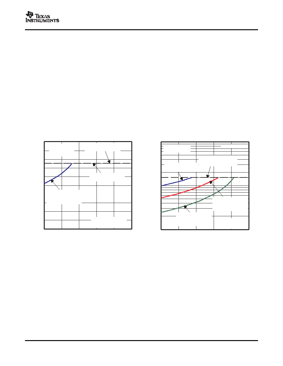
The next consideration is the package constraints. The two sources of heat within an amplifier are quiescent
power and output power. The designer should never forget about the quiescent heat generated within the device,
especially with multiamplifier devices. Because these devices have linear output stages (Class A-B), most of the
heat dissipation is at low output voltages with high output currents. Figure 40 through Figure 43 show this effect,
along with the quiescent heat, with an ambient air temperature of 50
°C. Obviously, as the ambient temperature
increases, the limit lines shown drop accordingly. The area under each respective limit line is considered the safe
operating area. Any condition above this line exceeds the amplifier limits and failure may result. When using VCC
= ±5 V, there is generally not a heat problem, even with SOIC packages. But, when using VCC = ±15 V, the SOIC
package is severely limited in the amount of heat it can dissipate. The other key factor when looking at these
graphs is how the devices are mounted on the PCB. The PowerPAD devices are extremely useful for heat
dissipation. But the device should always be soldered to a copper plane to use fully the heat dissipation
properties of the thermal pad. The SOIC package, on the other hand, is highly dependent on how it is mounted
on the PCB. As more trace and copper area is placed around the device,
θJA decreases and the heat dissipation
capability increases. The currents and voltages shown in these graphs are for the total package. For the
dual-amplifier package (THS4022), the sum of the RMS output currents and voltages should be used to choose
the proper package. The graphs shown assume that both amplifier outputs are identical.
THS4021
MAXIMUM RMS OUTPUT CURRENT
vs
RMS OUTPUT VOLTAGE DUE TO THERMAL LIMITS
Figure 40.
Figure 41.
Copyright 1999–2007, Texas Instruments Incorporated
17
相關PDF資料 |
PDF描述 |
|---|---|
| THS4022CDRG4 | 2 CHANNEL, VIDEO AMPLIFIER, PDSO8 |
| THS4022IDRG4 | 2 CHANNEL, VIDEO AMPLIFIER, PDSO8 |
| THS4021CDRG4 | 1 CHANNEL, VIDEO AMPLIFIER, PDSO8 |
| THS4061IDGN | 1 CHANNEL, VIDEO AMPLIFIER, PDSO8 |
| THS4061MFK | 1 CHANNEL, VIDEO AMPLIFIER, CQCC20 |
相關代理商/技術參數 |
參數描述 |
|---|---|
| THS4022CDR | 功能描述:高速運算放大器 350-MHz Low-Noise Vltg-Feedback Dual RoHS:否 制造商:Texas Instruments 通道數量:1 電壓增益 dB:116 dB 輸入補償電壓:0.5 mV 轉換速度:55 V/us 工作電源電壓:36 V 電源電流:7.5 mA 最大工作溫度:+ 85 C 安裝風格:SMD/SMT 封裝 / 箱體:SOIC-8 封裝:Tube |
| THS4022CDRG4 | 功能描述:高速運算放大器 350-MHz Low-Noise Vltg-Feedback Dual RoHS:否 制造商:Texas Instruments 通道數量:1 電壓增益 dB:116 dB 輸入補償電壓:0.5 mV 轉換速度:55 V/us 工作電源電壓:36 V 電源電流:7.5 mA 最大工作溫度:+ 85 C 安裝風格:SMD/SMT 封裝 / 箱體:SOIC-8 封裝:Tube |
| THS4022D | 制造商:TI 制造商全稱:Texas Instruments 功能描述:350-MHz LOW-NOISE HIGH-SPEED AMPLIFIERS |
| THS4022DGN | 制造商:TI 制造商全稱:Texas Instruments 功能描述:350-MHz LOW-NOISE HIGH-SPEED AMPLIFIERS |
| THS4022EVM | 功能描述:放大器 IC 開發工具 THS4022 Hi-Spd Amp Eval Mod RoHS:否 制造商:International Rectifier 產品:Demonstration Boards 類型:Power Amplifiers 工具用于評估:IR4302 工作電源電壓:13 V to 23 V |
發布緊急采購,3分鐘左右您將得到回復。