- 您現(xiàn)在的位置:買賣IC網(wǎng) > PDF目錄98226 > THS4223PWPR (TEXAS INSTRUMENTS INC) 3 CHANNEL, VIDEO PREAMPLIFIER, PDSO14 PDF資料下載
參數(shù)資料
| 型號: | THS4223PWPR |
| 廠商: | TEXAS INSTRUMENTS INC |
| 元件分類: | 音頻/視頻放大 |
| 英文描述: | 3 CHANNEL, VIDEO PREAMPLIFIER, PDSO14 |
| 封裝: | POWERPAD, PLASTIC, TSSOP-14 |
| 文件頁數(shù): | 10/32頁 |
| 文件大小: | 411K |
| 代理商: | THS4223PWPR |
第1頁第2頁第3頁第4頁第5頁第6頁第7頁第8頁第9頁當(dāng)前第10頁第11頁第12頁第13頁第14頁第15頁第16頁第17頁第18頁第19頁第20頁第21頁第22頁第23頁第24頁第25頁第26頁第27頁第28頁第29頁第30頁第31頁第32頁
THS4221, THS4225
THS4222, THS4226
THS4223, THS4227
SLOS399C – AUGUST 2002 – REVISED JANUARY 2003
www.ti.com
18
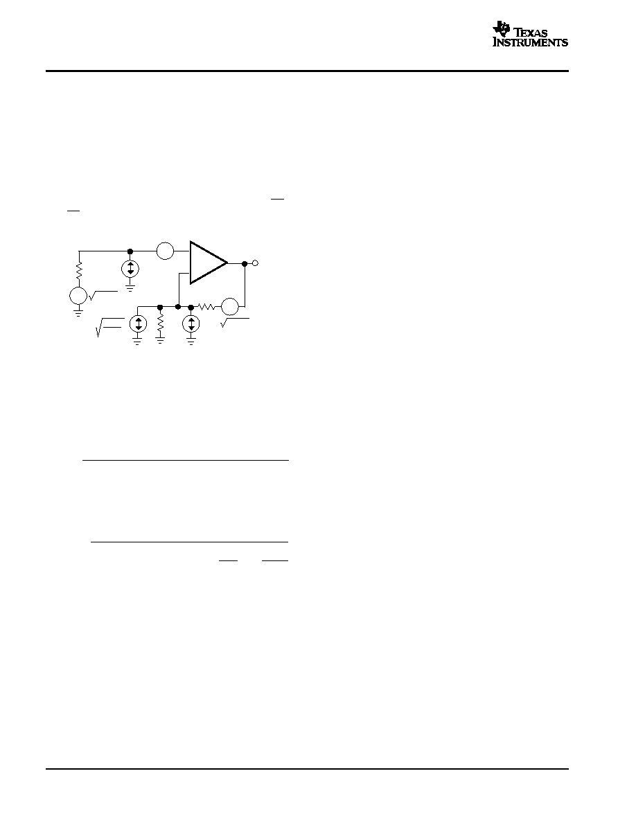
NOISE ANALYSIS
High slew rates, unity gain stable, voltage-feedback
operational amplifiers usually achieve their slew rate at the
expense of a higher input noise voltage. The input-referred
voltage noise, and the two input-referred current noise
terms, combine to give low output noise under a wide
variety of operating conditions. Figure 35 shows the
amplifier noise analysis model with all the noise terms
included. In this model, all noise terms are taken to be
noise voltage or current density terms in either nV/
√Hz or
pA/
√Hz.
_
+
Rf
4kT = 1.6E–20J
at 290K
THS4222 FAMILY
IBN
EO
ERF
RS
ERS
IBI
Rg
ENI
4kTRS
4kT
Rg
4kTRf
Figure 35. Noise Analysis Model
The total output shot noise voltage can be computed as the
square of all squares output noise voltage contributors.
Equation 1 shows the general form for the output noise
voltage using the terms shown in Figure 35:
E
O +
E 2
NI
) I
BNRS
2
) 4kTR
S NG
2
) I
BIRf
2
) 4kTR
fNG
Dividing this expression by the noise gain (NG=(1+ Rf/Rg))
gives the equivalent input-referred spot noise voltage at
the noninverting input, as shown in Equation 2:
E
O +
E 2
NI
) I
BNRS
2 ) 4kTR
S )
I
BIRf
NG
2
)
4kTR
f
NG
Driving Capacitive Loads
One of the most demanding, and yet very common, load
conditions for an op amp is capacitive loading. Often, the
capacitive load is the input of an A/D converter, including
additional
external
capacitance,
which
may
be
recommended to improve A/D linearity. A high-speed, high
open-loop gain amplifier like the THS4222 can be very
susceptible to decreased stability and closed-loop
response peaking when a capacitive load is placed directly
on the output pin. When the amplifier’s open-loop output
resistance is considered, this capacitive load introduces
an additional pole in the signal path that can decrease the
phase margin. When the primary considerations are
frequency response flatness, pulse response fidelity, or
distortion, the simplest and most effective solution is to
isolate the capacitive load from the feedback loop by
inserting a series isolation resistor between the amplifier
output and the capacitive load. This does not eliminate the
pole from the loop response, but rather shifts it and adds
a zero at a higher frequency. The additional zero acts to
cancel the phase lag from the capacitive load pole, thus
increasing the phase margin and improving stability.
BOARD LAYOUT
Achieving optimum performance with a high frequency
amplifier like the THS4222 requires careful attention to
board layout parasitics and external component types.
Recommendationsthat will optimize performance include:
1.
Minimize parasitic capacitance to any ac ground
for all of the signal I/O pins. Parasitic capacitance on
the output and inverting input pins can cause
instability: on the noninverting input, it can react with
the source impedance to cause unintentional band
limiting. To reduce unwanted capacitance, a window
around the signal I/O pins should be opened in all of
the ground and power planes around those pins.
Otherwise, ground and power planes should be
unbroken elsewhere on the board.
2.
Minimize the distance (< 0.25”) from the power
supply pins to high frequency 0.1-
F decoupling
capacitors. At the device pins, the ground and power
plane layout should not be in close proximity to the
signal I/O pins. Avoid narrow power and ground traces
to minimize inductance between the pins and the
decoupling capacitors. The power supply connections
should always be decoupled with these capacitors.
Larger (2.2-
F to 6.8-F) decoupling capacitors,
effective at lower frequency, should also be used on
the main supply pins. These may be placed somewhat
farther from the device and may be shared among
several devices in the same area of the PC board.
3.
Careful selection and placement of external
components will preserve the high frequency
performance of the THS4222. Resistors should be
a very low reactance type. Surface-mount resistors
work best and allow a tighter overall layout. Metal-film
and carbon composition, axially-leaded resistors can
also provide good high frequency performance.
Again, keep their leads and PC board trace length as
short as possible. Never use wire wound type
resistors in a high frequency application. Since the
output pin and inverting input pin are the most
sensitive to parasitic capacitance, always position the
feedback and series output resistor, if any, as close as
possible to the output pin. Other network components,
such as noninverting input termination resistors,
should also be placed close to the package. Where
double-side component mounting is allowed, place
(1)
(2)
相關(guān)PDF資料 |
PDF描述 |
|---|---|
| THS4223PWP | 3 CHANNEL, VIDEO PREAMPLIFIER, PDSO14 |
| THS4223DR | 3 CHANNEL, VIDEO PREAMPLIFIER, PDSO14 |
| THS4223D | 3 CHANNEL, VIDEO PREAMPLIFIER, PDSO14 |
| THS4227PWPR | 3 CHANNEL, VIDEO PREAMPLIFIER, PDSO16 |
| THS4227PWP | 3 CHANNEL, VIDEO PREAMPLIFIER, PDSO16 |
相關(guān)代理商/技術(shù)參數(shù) |
參數(shù)描述 |
|---|---|
| THS4225 | 制造商:TI 制造商全稱:Texas Instruments 功能描述:LOW-DISTORTION, HIGH-SPEED, RAIL-TO-RAIL OUTPUT OPERATIONAL AMPLIFIERS |
| THS4225D | 功能描述:高速運算放大器 Low-Distortion High Speed R-to-R Output RoHS:否 制造商:Texas Instruments 通道數(shù)量:1 電壓增益 dB:116 dB 輸入補償電壓:0.5 mV 轉(zhuǎn)換速度:55 V/us 工作電源電壓:36 V 電源電流:7.5 mA 最大工作溫度:+ 85 C 安裝風(fēng)格:SMD/SMT 封裝 / 箱體:SOIC-8 封裝:Tube |
| THS4225D | 制造商:Texas Instruments 功能描述:IC OP-AMP VFB R-R 120MHZ LV 8SOIC 制造商:Texas Instruments 功能描述:IC, OP-AMP VFB R-R 120MHZ LV 8SOIC 制造商:Texas Instruments 功能描述:IC, OP-AMP VFB R-R 120MHZ LV 8SOIC; Op Amp Type:Low Distortion; No. of Amplifiers:1; Slew Rate:975V/s; Supply Voltage Range: 1.35V to 7.5V; Amplifier Case Style:SOIC; No. of Pins:8; Bandwidth:230MHz; Operating Temperature ;RoHS Compliant: Yes |
| THS4225DG4 | 功能描述:高速運算放大器 Low-Distortion High Speed R-to-R Output RoHS:否 制造商:Texas Instruments 通道數(shù)量:1 電壓增益 dB:116 dB 輸入補償電壓:0.5 mV 轉(zhuǎn)換速度:55 V/us 工作電源電壓:36 V 電源電流:7.5 mA 最大工作溫度:+ 85 C 安裝風(fēng)格:SMD/SMT 封裝 / 箱體:SOIC-8 封裝:Tube |
| THS4225DGK | 功能描述:高速運算放大器 Low-Distortion High Speed R-to-R Output RoHS:否 制造商:Texas Instruments 通道數(shù)量:1 電壓增益 dB:116 dB 輸入補償電壓:0.5 mV 轉(zhuǎn)換速度:55 V/us 工作電源電壓:36 V 電源電流:7.5 mA 最大工作溫度:+ 85 C 安裝風(fēng)格:SMD/SMT 封裝 / 箱體:SOIC-8 封裝:Tube |
發(fā)布緊急采購,3分鐘左右您將得到回復(fù)。