- 您現在的位置:買賣IC網 > PDF目錄98227 > THS4271MDGNTEP (TEXAS INSTRUMENTS INC) 1 CHANNEL, VIDEO AMPLIFIER, PDSO8 PDF資料下載
參數資料
| 型號: | THS4271MDGNTEP |
| 廠商: | TEXAS INSTRUMENTS INC |
| 元件分類: | 音頻/視頻放大 |
| 英文描述: | 1 CHANNEL, VIDEO AMPLIFIER, PDSO8 |
| 封裝: | PLASTIC, MSOP-8 |
| 文件頁數: | 18/39頁 |
| 文件大小: | 915K |
| 代理商: | THS4271MDGNTEP |
第1頁第2頁第3頁第4頁第5頁第6頁第7頁第8頁第9頁第10頁第11頁第12頁第13頁第14頁第15頁第16頁第17頁當前第18頁第19頁第20頁第21頁第22頁第23頁第24頁第25頁第26頁第27頁第28頁第29頁第30頁第31頁第32頁第33頁第34頁第35頁第36頁第37頁第38頁第39頁
THS4271EP
THS4275EP
SGLS270B DECEMBER 2004 REVISED JULY 2008
www.ti.com
25
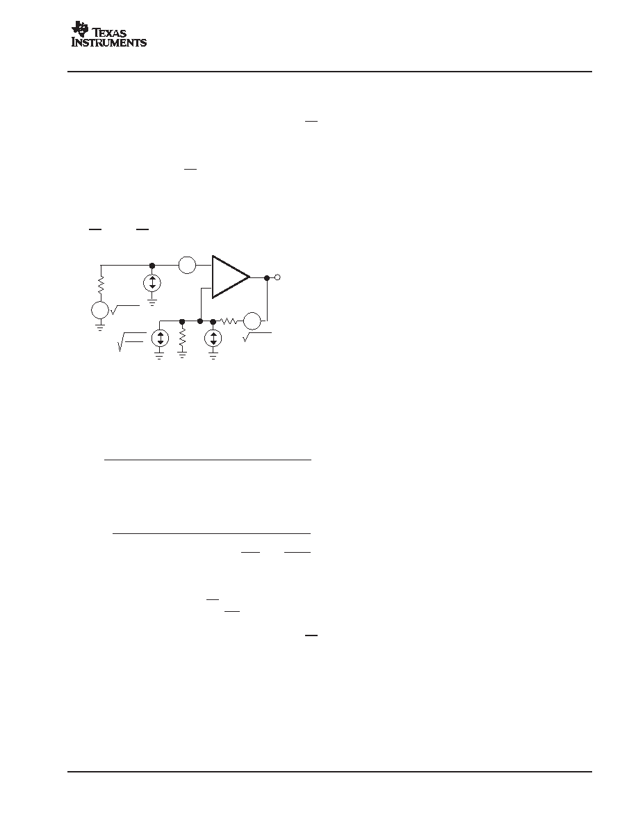
NOISE ANALYSIS
High slew rate, unity gain stable, voltage-feedback
operational amplifiers usually achieve their slew rate at the
expense of a higher input noise voltage. The 3-nV/
√Hz
input voltage noise for the THS4271 and THS4275 is,
however, much lower than comparable amplifiers. The
input-referred voltage noise, and the two input-referred
current noise terms (3 pA/
√Hz), combine to give low output
noise under a wide variety of operating conditions.
Figure 88 shows the amplifier noise analysis model with all
the noise terms included. In this model, all noise terms are
taken to be noise voltage or current density terms in either
nV/
√Hz or pA/√Hz.
_
+
Rf
4kT = 1.6E20J
at 290K
THS4271/THS4275
IBN
EO
ERF
RS
ERS
IBI
Rg
ENI
4kTRS
4kT
Rg
4kTRf
Figure 88. Noise Analysis Model
The total output shot noise voltage can be computed as the
square of all square output noise voltage contributors.
Equation 3 shows the general form for the output noise
voltage using the terms shown in Figure 88:
E
O +
E 2
NI
) I
BNRS
2
) 4kTR
S NG
2
) I
BIRf
2
) 4kTR
fNG
Dividing this expression by the noise gain (NG=(1+ Rf/Rg))
gives the equivalent input-referred spot noise voltage at
the noninverting input, as shown in Equation 4:
E
O +
E 2
NI
) I
BNRS
2 ) 4kTR
S )
I
BIRf
NG
2
)
4kTR
f
NG
Evaluation of these two equations for the circuit and
component values shown in Figure 76 gives a total output
spot noise voltage of 12.2 nV/
√Hz and a total equivalent
input spot noise voltage of 6.2 nV/
√Hz. This includes the
noise added by the resistors. This total input-referred spot
noise voltage is not much higher than the 3 nV/
√Hz
specification for the amplifier voltage noise alone.
Driving Capacitive Loads
One of the most demanding, and yet common, load
conditions for an op amp is capacitive loading. Often, the
capacitive load is the input of an A/D converter, including
additional
external
capacitance,
which
may
be
recommended to improve A/D linearity. A high-speed, high
open-loop gain amplifier like the THS4271 can be
susceptible to decreased stability and closed-loop
response peaking when a capacitive load is placed directly
on the output pin. When the amplifier’s open-loop output
resistance is considered, this capacitive load introduces
an additional pole in the signal path that can decrease the
phase margin. When the primary considerations are
frequency response flatness, pulse response fidelity, or
distortion, the simplest and most effective solution is to
isolate the capacitive load from the feedback loop by
inserting a series isolation resistor between the amplifier
output and the capacitive load. This does not eliminate the
pole from the loop response, but rather shifts it and adds
a zero at a higher frequency. The additional zero acts to
cancel the phase lag from the capacitive load pole, thus
increasing the phase margin and improving stability.
The Typical Characteristics show the recommended
isolation resistor vs capacitive load and the resulting
frequency response at the load. Parasitic capacitive loads
greater than 2 pF can begin to degrade the performance
of the THS4271. Long PC board traces, unmatched
cables, and connections to multiple devices can easily
cause this value to be exceeded. Always consider this
effect carefully, and add the recommended series resistor
as close as possible to the THS4271 output pin (see Board
Layout Guidelines).
The criterion for setting this R(ISO) resistor is a maximum
bandwidth, flat frequency response at the load. For a gain
of +2, the frequency response at the output pin is already
slightly peaked without the capacitive load, requiring
relatively high values of R(ISO) to flatten the response at
the load. Increasing the noise gain also reduces the
peaking.
(4)
(5)
相關PDF資料 |
PDF描述 |
|---|---|
| THS4271MDREP | 1 CHANNEL, VIDEO AMPLIFIER, PDSO8 |
| THS4275MDEP | 1 CHANNEL, VIDEO AMPLIFIER, PDSO8 |
| THS4275MDGNREP | 1 CHANNEL, VIDEO AMPLIFIER, PDSO8 |
| THS4275MDGNTEP | 1 CHANNEL, VIDEO AMPLIFIER, PDSO8 |
| THS4275MDREP | 1 CHANNEL, VIDEO AMPLIFIER, PDSO8 |
相關代理商/技術參數 |
參數描述 |
|---|---|
| THS4275D | 功能描述:高速運算放大器 Super-Fast Ultra-Low Distortion Hi-Speed RoHS:否 制造商:Texas Instruments 通道數量:1 電壓增益 dB:116 dB 輸入補償電壓:0.5 mV 轉換速度:55 V/us 工作電源電壓:36 V 電源電流:7.5 mA 最大工作溫度:+ 85 C 安裝風格:SMD/SMT 封裝 / 箱體:SOIC-8 封裝:Tube |
| THS4275DG4 | 功能描述:高速運算放大器 Super-Fast Ultra-Low Distortion Hi-Speed RoHS:否 制造商:Texas Instruments 通道數量:1 電壓增益 dB:116 dB 輸入補償電壓:0.5 mV 轉換速度:55 V/us 工作電源電壓:36 V 電源電流:7.5 mA 最大工作溫度:+ 85 C 安裝風格:SMD/SMT 封裝 / 箱體:SOIC-8 封裝:Tube |
| THS4275DGK | 功能描述:高速運算放大器 Super-Fast Ultra-Low Distortion Hi-Speed RoHS:否 制造商:Texas Instruments 通道數量:1 電壓增益 dB:116 dB 輸入補償電壓:0.5 mV 轉換速度:55 V/us 工作電源電壓:36 V 電源電流:7.5 mA 最大工作溫度:+ 85 C 安裝風格:SMD/SMT 封裝 / 箱體:SOIC-8 封裝:Tube |
| THS4275DGKG4 | 功能描述:高速運算放大器 Super-Fast Ultra-Low Distortion Hi-Speed RoHS:否 制造商:Texas Instruments 通道數量:1 電壓增益 dB:116 dB 輸入補償電壓:0.5 mV 轉換速度:55 V/us 工作電源電壓:36 V 電源電流:7.5 mA 最大工作溫度:+ 85 C 安裝風格:SMD/SMT 封裝 / 箱體:SOIC-8 封裝:Tube |
| THS4275DGKR | 功能描述:高速運算放大器 Super-Fast Ultra-Low Distortion Hi-Speed RoHS:否 制造商:Texas Instruments 通道數量:1 電壓增益 dB:116 dB 輸入補償電壓:0.5 mV 轉換速度:55 V/us 工作電源電壓:36 V 電源電流:7.5 mA 最大工作溫度:+ 85 C 安裝風格:SMD/SMT 封裝 / 箱體:SOIC-8 封裝:Tube |
發布緊急采購,3分鐘左右您將得到回復。