- 您現在的位置:買賣IC網 > PDF目錄98227 > THS4601CDDA (TEXAS INSTRUMENTS INC) 1 CHANNEL, VIDEO AMPLIFIER, PDSO8 PDF資料下載
參數資料
| 型號: | THS4601CDDA |
| 廠商: | TEXAS INSTRUMENTS INC |
| 元件分類: | 音頻/視頻放大 |
| 英文描述: | 1 CHANNEL, VIDEO AMPLIFIER, PDSO8 |
| 封裝: | GREEN, PLASTIC, SOP-8 |
| 文件頁數: | 5/34頁 |
| 文件大小: | 826K |
| 代理商: | THS4601CDDA |
第1頁第2頁第3頁第4頁當前第5頁第6頁第7頁第8頁第9頁第10頁第11頁第12頁第13頁第14頁第15頁第16頁第17頁第18頁第19頁第20頁第21頁第22頁第23頁第24頁第25頁第26頁第27頁第28頁第29頁第30頁第31頁第32頁第33頁第34頁
THS4601
SLOS388B OCTOBER 2001 REVISED JUNE 2002
13
www.ti.com
APPLICATION INFORMATION
designing the transimpedance circuit (continued)
As indicated, the current source typically sets the requirements for gain, speed, and dynamic range of the
amplifier. For a given amplifier and source combination, achievable performance is dictated by the following
parameters: the amplifier’s gain-bandwidth product, the amplifier’s input capacitance, the source capacitance,
the transimpedance gain, the amplifier’s slew rate, and the amplifier’s output swing. From this information, the
optimal performance of a transimpedance circuit using a given amplifier can be determined. Optimal is defined
here as providing the required transimpedance gain with a maximally flat frequency response.
For the circuit shown in Figure 26, all but one of the design parameters is known; the feedback capacitor must
be determined. Proper selection of the feedback capacitor prevents an unstable design, controls pulse
response characteristics, provides maximally flat transimpedance bandwidth, and limits broadband integrated
noise. The maximally flat frequency response results with CF calculated as shown in equation 1, where CF is
the feedback capacitor, RF is the feedback resistor, CS is the total source capacitance (including amplifier input
capacitance and parasitic capacitance at the inverting node), and GBP is the gain-bandwidth product of the
amplifier in hertz.
C
F +
1
pR
F
GBP
)
1
pR
F
GBP
2
)
4C
S
pR
F
GBP
2
Once the optimal feedback capacitor has been selected, the transimpedance bandwidth can be calculated with
equation 2.
F
–3 dB +
GBP
2
pR
F CS )
C
F
_
+
CIDIFF
CICM
CP
RF
CF
CD
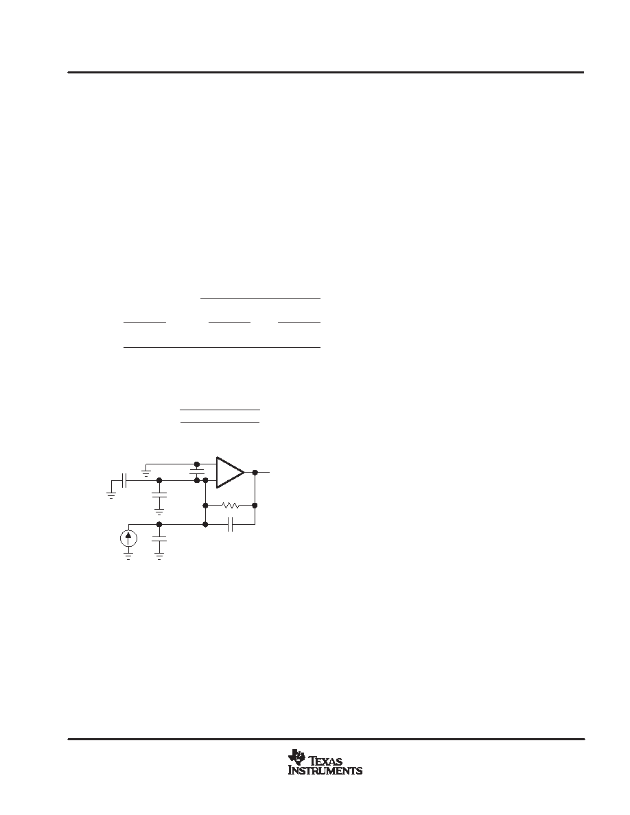
IDIODE
NOTE: The total source capacitance is the sum of several distinct capacitances.
Cs = CICM + CIDIFF + CP + CD
Where: CICM is the common-mode input capacitance.
CIDIFF is the differential input capacitance.
CD is the diode capacitance.
CP is parasitic capacitance at the inverting node.
Figure 27. Transimpedance Analysis Circuit
(1)
(2)
相關PDF資料 |
PDF描述 |
|---|---|
| THS4601CDR | 1 CHANNEL, VIDEO AMPLIFIER, PDSO8 |
| THS4601CD | 1 CHANNEL, VIDEO AMPLIFIER, PDSO8 |
| THS4601IDDAR | 1 CHANNEL, VIDEO AMPLIFIER, PDSO8 |
| THS4601IDDA | 1 CHANNEL, VIDEO AMPLIFIER, PDSO8 |
| THS4601IDR | 1 CHANNEL, VIDEO AMPLIFIER, PDSO8 |
相關代理商/技術參數 |
參數描述 |
|---|---|
| THS4601CDDAG3 | 功能描述:高速運算放大器 Wideband FET-Input Op Amp RoHS:否 制造商:Texas Instruments 通道數量:1 電壓增益 dB:116 dB 輸入補償電壓:0.5 mV 轉換速度:55 V/us 工作電源電壓:36 V 電源電流:7.5 mA 最大工作溫度:+ 85 C 安裝風格:SMD/SMT 封裝 / 箱體:SOIC-8 封裝:Tube |
| THS4601CDDAR | 功能描述:高速運算放大器 Wideband FET-Input Op Amp RoHS:否 制造商:Texas Instruments 通道數量:1 電壓增益 dB:116 dB 輸入補償電壓:0.5 mV 轉換速度:55 V/us 工作電源電壓:36 V 電源電流:7.5 mA 最大工作溫度:+ 85 C 安裝風格:SMD/SMT 封裝 / 箱體:SOIC-8 封裝:Tube |
| THS4601CDDARG3 | 功能描述:高速運算放大器 Wideband FET-Input Op Amp RoHS:否 制造商:Texas Instruments 通道數量:1 電壓增益 dB:116 dB 輸入補償電壓:0.5 mV 轉換速度:55 V/us 工作電源電壓:36 V 電源電流:7.5 mA 最大工作溫度:+ 85 C 安裝風格:SMD/SMT 封裝 / 箱體:SOIC-8 封裝:Tube |
| THS4601CDG4 | 功能描述:高速運算放大器 Wideband FET-Input Op Amp RoHS:否 制造商:Texas Instruments 通道數量:1 電壓增益 dB:116 dB 輸入補償電壓:0.5 mV 轉換速度:55 V/us 工作電源電壓:36 V 電源電流:7.5 mA 最大工作溫度:+ 85 C 安裝風格:SMD/SMT 封裝 / 箱體:SOIC-8 封裝:Tube |
| THS4601EVM | 功能描述:放大器 IC 開發工具 THS4601 Eval Mod RoHS:否 制造商:International Rectifier 產品:Demonstration Boards 類型:Power Amplifiers 工具用于評估:IR4302 工作電源電壓:13 V to 23 V |
發布緊急采購,3分鐘左右您將得到回復。