- 您現在的位置:買賣IC網 > PDF目錄98227 > THS5641AIPWR (TEXAS INSTRUMENTS INC) PARALLEL, 8 BITS INPUT LOADING, 0.035 us SETTLING TIME, 8-BIT DAC, PDSO28 PDF資料下載
參數資料
| 型號: | THS5641AIPWR |
| 廠商: | TEXAS INSTRUMENTS INC |
| 元件分類: | DAC |
| 英文描述: | PARALLEL, 8 BITS INPUT LOADING, 0.035 us SETTLING TIME, 8-BIT DAC, PDSO28 |
| 封裝: | GREEN, PLASTIC, TSSOP-28 |
| 文件頁數: | 23/31頁 |
| 文件大小: | 915K |
| 代理商: | THS5641AIPWR |
第1頁第2頁第3頁第4頁第5頁第6頁第7頁第8頁第9頁第10頁第11頁第12頁第13頁第14頁第15頁第16頁第17頁第18頁第19頁第20頁第21頁第22頁當前第23頁第24頁第25頁第26頁第27頁第28頁第29頁第30頁第31頁
THS5641A
8BIT, 100 MSPS, CommsDAC
DIGITALTOANALOG CONVERTER
SLAS277A MARCH 2000 REVISED SEPTEMBER 2002
3
POST OFFICE BOX 655303
DALLAS, TEXAS 75265
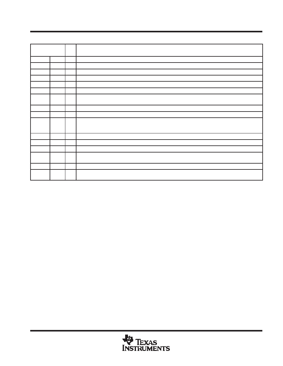
Terminal Functions
TERMINAL
I/O
DESCRIPTION
NAME
NO.
I/O
DESCRIPTION
AGND
20
I
Analog ground return for the internal analog circuitry
AVDD
24
I
Positive analog supply voltage (3 V to 5.5 V)
BIASJ
18
O
Full-scale output current bias
CLK
28
I
External clock input. Input data latched on rising edge of the clock.
COMP1
19
I
Compensation and decoupling node, requires a 0.1
F capacitor to AVDD.
COMP2
23
I
Internal bias node, requires a 0.1
F decoupling capacitor to AGND.
D[7:0]
[1:8]
I
Data bits 0 through 7.
D7 is most significant data bit (MSB), D0 is least significant data bit (LSB).
DGND
26
I
Digital ground return for the internal digital logic circuitry
DVDD
27
I
Positive digital supply voltage (3 V to 5.5 V)
EXTIO
17
I/O
Used as external reference input when internal reference is disabled (i.e., EXTLO = AVDD). Used as internal
reference output when EXTLO = AGND, requires a 0.1
F decoupling capacitor to AGND when used as reference
output
EXTLO
16
O
Internal reference ground. Connect to AVDD to disable the internal reference source
IOUT1
22
O
DAC current output. Full scale when all input bits are set 1
IOUT2
21
O
Complementary DAC current output. Full scale when all input bits are 0
MODE
25
I
Mode select. Internal pulldown. Mode 0 is selected if this pin is left floating or connected to DGND. See
timing diagram.
NC
[9:14]
N
No connection
SLEEP
15
I
Asynchronous hardware power down input. Active High. Internal pulldown. Requires 5
s to power down but 3 ms
to power up.
absolute maximum ratings over operating free-air temperature (unless otherwise noted)
Supply voltage range, AVDD (see Note 1)
0.3 V to 6.5 V
. . . . . . . . . . . . . . . . . . . . . . . . . . . . . . . . . . . . . . . . . . . .
DVDD (see Note 2)
0.3 V to 6.5 V
. . . . . . . . . . . . . . . . . . . . . . . . . . . . . . . . . . . . . . . . . . .
Voltage between AGND and DGND
0.3 V to 0.5 V
. . . . . . . . . . . . . . . . . . . . . . . . . . . . . . . . . . . . . . . . . . . . . . . . .
Supply voltage range, AVDD to DVDD
6.5 V to 6.5 V
. . . . . . . . . . . . . . . . . . . . . . . . . . . . . . . . . . . . . . . . . . . . . . .
CLK, SLEEP, MODE (see Note 2)
0.3 V to DVDD + 0.3 V
. . . . . . . . . . . . . . . . . . . . . .
Digital input D7D0 (see Note 2)
0.3 V to DVDD + 0.3 V
. . . . . . . . . . . . . . . . . . . . . .
IOUT1, IOUT2 (see Note 1)
1 V to AVDD + 0.3 V
. . . . . . . . . . . . . . . . . . . . . . . . . . . . . .
COMP1, COMP2 (see Note 1)
0.3 V to AVDD + 0.3 V
. . . . . . . . . . . . . . . . . . . . . . . . .
EXTIO, BIASJ (see Note 1)
0.3 V to AVDD + 0.3 V
. . . . . . . . . . . . . . . . . . . . . . . . . . . .
EXTLO (see Note 1)
0.3 V to 0.3 V
. . . . . . . . . . . . . . . . . . . . . . . . . . . . . . . . . . . . . . . . . .
Peak input current (any input)
20 mA
. . . . . . . . . . . . . . . . . . . . . . . . . . . . . . . . . . . . . . . . . . . . . . . . . . . . . . . . . . . . .
Peak total input current (all inputs)
30 mA
. . . . . . . . . . . . . . . . . . . . . . . . . . . . . . . . . . . . . . . . . . . . . . . . . . . . . . . .
Operating free-air temperature range, TA: THS5641AI
40
°C to 85°C
. . . . . . . . . . . . . . . . . . . . . . . . . . . . . . . . .
Storage temperature range
65
°C to 150°C
. . . . . . . . . . . . . . . . . . . . . . . . . . . . . . . . . . . . . . . . . . . . . . . . . . . . . . . .
Lead temperature 1,6 mm (1/16 inch) from the case for 10 seconds
260
°C
. . . . . . . . . . . . . . . . . . . . . . . . . . . .
Stresses beyond those listed under “absolute maximum ratings” may cause permanent damage to the device. These are stress ratings only, and
functional operation of the device at these or any other conditions beyond those indicated under “recommended operating conditions” is not
implied. Exposure to absolute-maximum-rated conditions for extended periods may affect device reliability.
NOTES:
1. Measured with respect to AGND.
2. Measured with respect to DGND.
相關PDF資料 |
PDF描述 |
|---|---|
| THS5641AIDWRG4 | PARALLEL, 8 BITS INPUT LOADING, 0.035 us SETTLING TIME, 8-BIT DAC, PDSO28 |
| THS5641AIDWG4 | PARALLEL, 8 BITS INPUT LOADING, 0.035 us SETTLING TIME, 8-BIT DAC, PDSO28 |
| THS5641AIPWRG4 | PARALLEL, 8 BITS INPUT LOADING, 0.035 us SETTLING TIME, 8-BIT DAC, PDSO28 |
| THS5641AIDWR | PARALLEL, 8 BITS INPUT LOADING, 0.035 us SETTLING TIME, 8-BIT DAC, PDSO28 |
| THS5641IDWR | PARALLEL, 8 BITS INPUT LOADING, 0.035 us SETTLING TIME, 8-BIT DAC, PDSO28 |
相關代理商/技術參數 |
參數描述 |
|---|---|
| THS5641AIPWRG4 | 功能描述:數模轉換器- DAC 8-Bit 100 MSPS CommsDAC RoHS:否 制造商:Texas Instruments 轉換器數量:1 DAC 輸出端數量:1 轉換速率:2 MSPs 分辨率:16 bit 接口類型:QSPI, SPI, Serial (3-Wire, Microwire) 穩定時間:1 us 最大工作溫度:+ 85 C 安裝風格:SMD/SMT 封裝 / 箱體:SOIC-14 封裝:Tube |
| THS5641APW | 制造商:TI 制造商全稱:Texas Instruments 功能描述:8-BIT, 100 MSPS, CommsDACE DIGITAL-TO-ANALOG CONVERTER |
| THS5641DW | 制造商:TI 制造商全稱:Texas Instruments 功能描述:8-BIT, 100 MSPS, CommsDACE DIGITAL-TO-ANALOG CONVERTER |
| THS5641EVM | 功能描述:數據轉換 IC 開發工具 THS5641 Eval Mod RoHS:否 制造商:Texas Instruments 產品:Demonstration Kits 類型:ADC 工具用于評估:ADS130E08 接口類型:SPI 工作電源電壓:- 6 V to + 6 V |
| THS5641IDW | 功能描述:IC 8-BIT 100MSPS D/A 28-SOIC RoHS:否 類別:集成電路 (IC) >> 數據采集 - 數模轉換器 系列:CommsDAC™ 產品培訓模塊:Data Converter Fundamentals DAC Architectures 標準包裝:3,000 系列:nanoDAC™ 設置時間:80µs 位數:18 數據接口:DSP,MICROWIRE?,QSPI?,串行,SPI? 轉換器數目:1 電壓電源:單電源 功率耗散(最大):- 工作溫度:-40°C ~ 105°C 安裝類型:表面貼裝 封裝/外殼:SOT-23-8 供應商設備封裝:SOT-23-8 包裝:帶卷 (TR) 輸出數目和類型:1 電壓,單極 采樣率(每秒):- 產品目錄頁面:784 (CN2011-ZH PDF) 配用:EVAL-AD5680EBZ-ND - BOARD EVAL FOR AD5680 其它名稱:AD5680BRJZ-2REEL7TR |
發布緊急采購,3分鐘左右您將得到回復。