- 您現(xiàn)在的位置:買賣IC網(wǎng) > PDF目錄98228 > THS5661IPW (TEXAS INSTRUMENTS INC) PARALLEL, WORD INPUT LOADING, 0.035 us SETTLING TIME, 12-BIT DAC, PDSO28 PDF資料下載
參數(shù)資料
| 型號: | THS5661IPW |
| 廠商: | TEXAS INSTRUMENTS INC |
| 元件分類: | DAC |
| 英文描述: | PARALLEL, WORD INPUT LOADING, 0.035 us SETTLING TIME, 12-BIT DAC, PDSO28 |
| 封裝: | PLASTIC, TSSOP-28 |
| 文件頁數(shù): | 1/30頁 |
| 文件大小: | 778K |
| 代理商: | THS5661IPW |
當(dāng)前第1頁第2頁第3頁第4頁第5頁第6頁第7頁第8頁第9頁第10頁第11頁第12頁第13頁第14頁第15頁第16頁第17頁第18頁第19頁第20頁第21頁第22頁第23頁第24頁第25頁第26頁第27頁第28頁第29頁第30頁
THS5661
12-BIT, 100 MSPS, CommsDAC
DIGITAL-TO-ANALOG CONVERTER
SLAS200A – MAY 1999 – REVISED JULY 1999
1
POST OFFICE BOX 655303
DALLAS, TEXAS 75265
D Member of the Pin-Compatible
CommsDAC
Product Family
D 100 MSPS Update Rate
D 12-Bit Resolution
D Spurious Free Dynamic Range (SFDR) to
Nyquist at 20 MHz Output: 63 dBc
D 1 ns Setup/Hold Time
D Differential Scalable Current Outputs: 2 mA
to 20 mA
D On-Chip 1.2 V Reference
D 3 V and 5 V CMOS-Compatible Digital
Interface
D Straight Binary or Twos Complement Input
D Power Dissipation: 175 mW at 5 V, Sleep
Mode: 25 mW at 5 V
D Package: 28-Pin SOIC and TSSOP
description
The THS5661 is a 12-bit resolution digital-to-analog converter (DAC) specifically optimized for digital data
transmission in wired and wireless communication systems. The 12-bit DAC is a member of the CommsDAC
series of high-speed, low-power CMOS digital-to-analog converters. The CommsDAC family consists of pin
compatible 14-, 12-, 10-, and 8-bit DACs. All devices offer identical interface options, small outline package, and
pinout. The THS5661 offers superior ac and dc performance while supporting update rates up to 100 MSPS.
The THS5661 operates from an analog supply of 4.5 V to 5.5 V. Its inherent low power dissipation of 175 mW
ensures that the device is well-suited for portable and low-power applications. Lowering the full-scale current
output reduces the power dissipation without significantly degrading performance. The device features a
SLEEP mode, which reduces the standby power to approximately 25 mW, thereby optimizing the power
consumption for system needs.
The THS5661 is manufactured in Texas Instruments advanced high-speed mixed-signal CMOS process. A
current-source-array architecture combined with simultaneous switching shows excellent dynamic
performance. On-chip edge-triggered input latches and a 1.2 V temperature-compensated bandgap reference
provide a complete monolithic DAC solution. The digital supply range of 3 V to 5.5 V supports 3 V and 5 V CMOS
logic families. Minimum data input setup and hold times allow for easy interfacing with external logic. The
THS5661 supports both a straight binary and twos complement input word format, enabling flexible interfacing
with digital signal processors.
The THS5661 provides a nominal full-scale differential output current of 20 mA and >300 k
output impedance,
supporting both single-ended and differential applications. The output current can be directly fed to the load
(e.g., external resistor load or transformer), with no additional external output buffer required. An accurate
on-chip reference and control amplifier allows the user to adjust this output current from 20 mA down to 2 mA,
with no significant degradation of performance. This reduces power consumption and provides 20 dB gain range
control capabilities. Alternatively, an external reference voltage and control amplifier may be applied in
applications using a multiplying DAC. The output voltage compliance range is 1.25 V.
Copyright
1999, Texas Instruments Incorporated
PRODUCTION DATA information is current as of publication date.
Products conform to specifications per the terms of Texas Instruments
standard warranty. Production processing does not necessarily include
testing of all parameters.
Please be aware that an important notice concerning availability, standard warranty, and use in critical applications of
Texas Instruments semiconductor products and disclaimers thereto appears at the end of this data sheet.
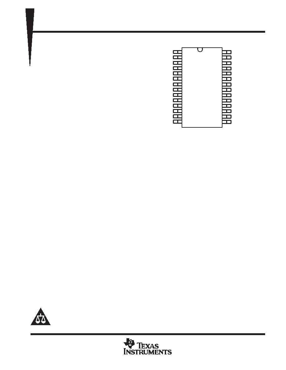
1
2
3
4
5
6
7
8
9
10
11
12
13
14
28
27
26
25
24
23
22
21
20
19
18
17
16
15
D11
D10
D9
D8
D7
D6
D5
D4
D3
D2
D1
D0
NC
CLK
DVDD
DGND
MODE
AVDD
COMP2
IOUT1
IOUT2
AGND
COMP1
BIASJ
EXTIO
EXTLO
SLEEP
SOIC (DW) OR TSSOP (PW) PACKAGE
(TOP VIEW)
NC – No internal connection
CommsDAC is a trademark of Texas Instruments Incorporated.
相關(guān)PDF資料 |
PDF描述 |
|---|---|
| THS5661IPWR | PARALLEL, WORD INPUT LOADING, 0.035 us SETTLING TIME, 12-BIT DAC, PDSO28 |
| THS5661IDWR | PARALLEL, WORD INPUT LOADING, 0.035 us SETTLING TIME, 12-BIT DAC, PDSO28 |
| THS5661IDW | PARALLEL, WORD INPUT LOADING, 0.035 us SETTLING TIME, 12-BIT DAC, PDSO28 |
| THS5671AIDWRG4 | PARALLEL, WORD INPUT LOADING, 0.035 us SETTLING TIME, 14-BIT DAC, PDSO28 |
| THS5671AIPW | PARALLEL, WORD INPUT LOADING, 0.035 us SETTLING TIME, 14-BIT DAC, PDSO28 |
相關(guān)代理商/技術(shù)參數(shù) |
參數(shù)描述 |
|---|---|
| THS5661PW | 制造商:TI 制造商全稱:Texas Instruments 功能描述:12-BIT, 100 MSPS, CommsDACE DIGITAL-TO-ANALOG CONVERTER |
| THS5671A | 制造商:TI 制造商全稱:Texas Instruments 功能描述:14-BIT, 125 MSPS, CommsDAC DIGITAL-TO-ANALOG CONVERTER |
| THS5671ADW | 制造商:TI 制造商全稱:Texas Instruments 功能描述:14-BIT, 125 MSPS, CommsDAC DIGITAL-TO-ANALOG CONVERTER |
| THS5671AIDW | 功能描述:數(shù)模轉(zhuǎn)換器- DAC 14-Bit 125 MSPS CommsDAC RoHS:否 制造商:Texas Instruments 轉(zhuǎn)換器數(shù)量:1 DAC 輸出端數(shù)量:1 轉(zhuǎn)換速率:2 MSPs 分辨率:16 bit 接口類型:QSPI, SPI, Serial (3-Wire, Microwire) 穩(wěn)定時(shí)間:1 us 最大工作溫度:+ 85 C 安裝風(fēng)格:SMD/SMT 封裝 / 箱體:SOIC-14 封裝:Tube |
| THS5671AIDW | 制造商:Texas Instruments 功能描述:IC 14BIT DAC 125MSPS SMD |
發(fā)布緊急采購,3分鐘左右您將得到回復(fù)。