- 您現在的位置:買賣IC網 > PDF目錄98230 > TK65130MTL (ASAHI KASEI POWER DEVICES CORP) SWITCHING REGULATOR, 102 kHz SWITCHING FREQ-MAX, PDSO6 PDF資料下載
參數資料
| 型號: | TK65130MTL |
| 廠商: | ASAHI KASEI POWER DEVICES CORP |
| 元件分類: | 穩壓器 |
| 英文描述: | SWITCHING REGULATOR, 102 kHz SWITCHING FREQ-MAX, PDSO6 |
| 封裝: | SOT-23L, SMT-6 |
| 文件頁數: | 5/20頁 |
| 文件大小: | 158K |
| 代理商: | TK65130MTL |
January 2001 TOKO, Inc.
Page 13
TK651xxM
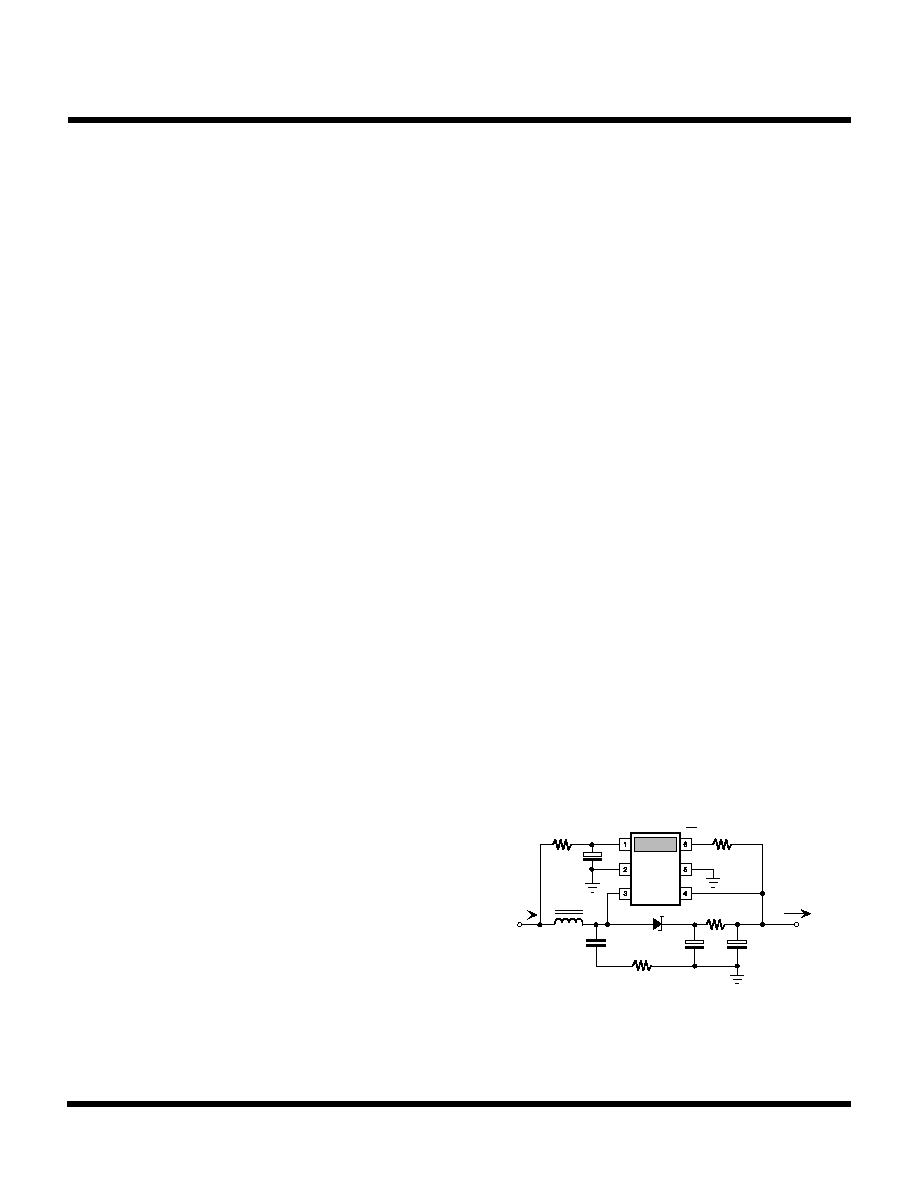
FIGURE 2: FILTERED TEST CIRCUIT
SINGLE-CELL APPLICATION (CONT.)
2) if the same battery is powering the TK651xx at the V
IN pin
(i.e., the normal case), then the IC may become inoperable
due to insufficient V
IN. This is why the application test circuit
features an RC filter into the V
IN pin. The current draw is
very small, so the voltage drop across this filter resistor is
negligible. The filter serves to average out the input ripple
caused by the battery resistance. Note that this filter is
optional, and the net effect of its use is the extension of
battery life by allowing the battery to be discharged more
deeply.
A more power-efficient method comes at the price of a large
capacitor. This can be placed in parallel with the battery to
help channel the converter current pulses away from the
battery. The capacitor must have low ESR compared to the
battery resistance in order to accomplish this effectively.
Still another solution is to filter the DC input with an LC filter.
However, it is more likely that the filter will be either too
large or too lossy. It is of questionable benefit to smooth the
input if the DC loss through the filter is large.
Assuming that input ripple voltage at the battery terminal
and converter input is large, and that we filter the V
IN pin of
the IC as in the test circuit, then the parameter “V
IN” in the
previous equations is not usable, and we will need to use
parameters to represent both the source voltage
and the
source resistance.
SWITCH ON-RESISTANCE, INDUCTOR WINDING
RESISTANCE, AND CAPACITANCE ESR
The on-resistance of the TK651xx’s internal switch is about
1 Ohm maximum. Using the previously stated example of
100 mA peak current, the voltage drop across the switch
would reach 100 mV during the on-time. This subtracts
from the voltage which is impressed across the inductor to
store energy during the on-time. As a result, less energy
is delivered to the output during the off-time.
If the winding resistance of the inductor increases to 1 Ohm
or greater, the voltage drop across the winding resistance
also subtracts from the voltage used to store energy in the
core. Thus, efficiency degradation occurs.
As the inductor delivers energy into the output capacitor
during the off-time, its current decays at a rate proportional
to the voltage drop across it. The idealized equations
assume that the voltage at the switching node is clamped
at a diode drop above the output voltage. However, the
ESR of the output capacitor can increase the voltage drop
across the inductor by the additional voltage dropped
across the ESR when the peak current flows in it. For
example, the voltage across a capacitor with an ESR of 2
Ohms (not unusual at cold temperature) would jump by 200
mV when 100 mA peak current began to flow in it. This extra
voltage drop would cause the inductor current to ramp
down more quickly, thus depleting the available output
current. Possible choices for low ESR capacitors are:
Panasonic TE series (surface mount); AVX TPS series
(surface mount); Matsuo 267 series (surface mount); Sanyo
OS-CON series.
LOI FEATURES
The Low Output Indicator (LOI) output can provide a reset
signal to a microprocessor or other external system
controller. When the output voltage falls below the LOI
threshold (during start-up of the converter or under a
current overload fault condition), the LOI signal is asserted
low, indicating that the system controller (i.e.,
microprocessor) should be in a reset mode. This method of
reset control can be used to prevent improper system
operation which might occur at low supply voltage levels.
The LOI threshold voltage is between 87% and 93% of the
regulated output voltage value. The LOI threshold also has
about 45 mV hysteresis between its on-off trigger levels.
RIPPLE AND NOISE CONSIDERATIONS
The filtered test circuit of the TK651xx is shown below in
Figure 2.
VIN
300 k
GND
LOI
VOUT
SW
IB
L = 95 H
D
IOUT
VOUT
RN
1 K
RS
1 K
VIN
CN
10 F
CD
10 F
CS
220 pF
ROF
15
+
CU
10 F
相關PDF資料 |
PDF描述 |
|---|---|
| TK750003DMG | SWITCHING CONTROLLER, 115 kHz SWITCHING FREQ-MAX, PDIP8 |
| TK75001DI | SWITCHING CONTROLLER, PDIP8 |
| TK75001DMG | SWITCHING CONTROLLER, 63 kHz SWITCHING FREQ-MAX, PDIP8 |
| TK75001UITL | SWITCHING CONTROLLER, 1000 kHz SWITCHING FREQ-MAX, PDSO5 |
| TK75001UIMG | SWITCHING CONTROLLER, 1000 kHz SWITCHING FREQ-MAX, PDSO5 |
相關代理商/技術參數 |
參數描述 |
|---|---|
| TK65130MTL/30M | 制造商:TOKO 制造商全稱:TOKO, Inc 功能描述:STEP-UP VOLTAGE CONVERTER WITH VOLTAGE MONITOR |
| TK65133 | 制造商:TOKO 制造商全稱:TOKO, Inc 功能描述:STEP-UP VOLTAGE CONVERTER WITH VOLTAGE MONITOR |
| TK65133M | 制造商:TOKO 制造商全稱:TOKO, Inc 功能描述:STEP-UP VOLTAGE CONVERTER WITH VOLTAGE MONITOR |
| TK65133MTL | 制造商:TOKO 制造商全稱:TOKO, Inc 功能描述:STEP-UP VOLTAGE CONVERTER WITH VOLTAGE MONITOR |
| TK65133MTL/33M | 制造商:TOKO 制造商全稱:TOKO, Inc 功能描述:STEP-UP VOLTAGE CONVERTER WITH VOLTAGE MONITOR |
發布緊急采購,3分鐘左右您將得到回復。