- 您現(xiàn)在的位置:買賣IC網(wǎng) > PDF目錄98234 > TLC1225INW (TEXAS INSTRUMENTS INC) 1-CH 12-BIT SUCCESSIVE APPROXIMATION ADC, PARALLEL ACCESS, PDIP28 PDF資料下載
參數(shù)資料
| 型號: | TLC1225INW |
| 廠商: | TEXAS INSTRUMENTS INC |
| 元件分類: | ADC |
| 英文描述: | 1-CH 12-BIT SUCCESSIVE APPROXIMATION ADC, PARALLEL ACCESS, PDIP28 |
| 封裝: | PLASTIC, DIP-28 |
| 文件頁數(shù): | 10/15頁 |
| 文件大小: | 230K |
| 代理商: | TLC1225INW |
TLC1225I, TLC1225M
SELF-CALIBRATING 12-BIT-PLUS-SIGN
ANALOG-TO-DIGITAL CONVERTERS
SLAS029B – AUGUST 1990 – REVISED DECEMBER 1993
4
POST OFFICE BOX 655303
DALLAS, TEXAS 75265
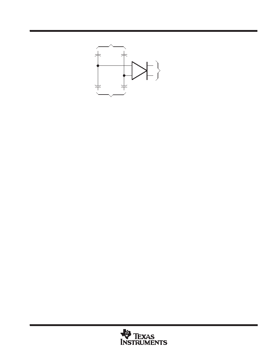
Vref (step 4)
GND (step 3)
GND (step 4)
Vref (step 3)
MSB-Capacitor
Voltage Error
(step 4)
CX
CMSB –
CX
CMSB +
Figure 2. Capacitor Array Null
analog-to-digital conversion
The following steps are performed in the analog-to-digital conversion process:
Step 1 of the calibration of comparator offset sequence is performed. The A/D conversion result for the
remaining comparator offset, obtained in step 2 of the calibration of comparator offset, is retrieved from
the RAM and is input to the 8-bit DACs. The comparator offset is completely corrected.
IN+ and IN– are sampled into the 13-bit capacitive arrays.
The 13-bit analog-to-digital conversion is performed. As the successive-approximation conversion
proceeds successively through the seven most significant capacitors, the error for each of these
capacitors is recovered from the RAM and accumulated in a register. This register controls the 8-bit
DACs so the total accumulated error for these capacitors is subtracted out during the conversion
process.
absolute maximum ratings over operating free-air temperature range (unless otherwise noted)
Supply voltage (ANLG VCC+ and DGTL VCC) (see Note 1)
7.5 V
. . . . . . . . . . . . . . . . . . . . . . . . . . . . . . . . . . . . .
Supply voltage, ANLG VCC–
– 7.5 V
. . . . . . . . . . . . . . . . . . . . . . . . . . . . . . . . . . . . . . . . . . . . . . . . . . . . . . . . . . . . . .
Differential supply voltage, ANLG VCC+ – ANLG VCC–
15 V
. . . . . . . . . . . . . . . . . . . . . . . . . . . . . . . . . . . . . . . .
Clock input voltage range
– 0.3 V to VCC + 0.3 V
. . . . . . . . . . . . . . . . . . . . . . . . . . . . . . . . . . . . . . . . . . . . . . . . . . .
Control input voltage range
– 0.3 V to VCC + 0.3 V
. . . . . . . . . . . . . . . . . . . . . . . . . . . . . . . . . . . . . . . . . . . . . . . . . .
Analog input (IN +, IN –) voltage range, VI+ and VI–
ANLG VCC– –0.3 V to ANLG VCC+ +0.3 V
. . . . . . . . .
Reference voltage range, Vref
– 0.3 V to ANLG VCC+ +0.3 V
. . . . . . . . . . . . . . . . . . . . . . . . . . . . . . . . . . . . . . . .
Voltage range, TIE HIGH
– 0.3 V to ANLG VCC+ +0.3 V
. . . . . . . . . . . . . . . . . . . . . . . . . . . . . . . . . . . . . . . . . . . .
Output voltage range
– 0.3 V to DGTL VCC +0.3 V
. . . . . . . . . . . . . . . . . . . . . . . . . . . . . . . . . . . . . . . . . . . . . . . . .
Input current (per pin)
±5 mA
. . . . . . . . . . . . . . . . . . . . . . . . . . . . . . . . . . . . . . . . . . . . . . . . . . . . . . . . . . . . . . . . . . . .
Input current (per package)
±20 mA
. . . . . . . . . . . . . . . . . . . . . . . . . . . . . . . . . . . . . . . . . . . . . . . . . . . . . . . . . . . . .
Continued total dissipation
See Dissipation Rating Table
. . . . . . . . . . . . . . . . . . . . . . . . . . . . . . . . . . . . . . . . . . . .
Operating free-air temperature range, TA: TLC1225I
– 40
°C to 85°C
. . . . . . . . . . . . . . . . . . . . . . . . . . . . . . . . . . .
TLC1225M
– 55
°C to 125°C
. . . . . . . . . . . . . . . . . . . . . . . . . . . . . . . .
Storage temperature range
– 65
°C to 150°C
. . . . . . . . . . . . . . . . . . . . . . . . . . . . . . . . . . . . . . . . . . . . . . . . . . . . . . .
Case temperature for 60 seconds: FK or FN package
260
°C
. . . . . . . . . . . . . . . . . . . . . . . . . . . . . . . . . . . . . . . . .
Lead temperature 1,6 mm (1/16 inch) from the case for 10 seconds: NW package
260
°C
. . . . . . . . . . . . . . . .
Lead temperature 1,6 mm (1/16 inch) from the case for 60 seconds: J package
300
°C
. . . . . . . . . . . . . . . . . .
Stresses beyond those listed under “absolute maximum ratings” may cause permanent damage to the device. These are stress ratings only, and
functional operation of the device at these or any other conditions beyond those indicated under “recommended operating conditions” is not
implied. Exposure to absolute-maximum-rated conditions for extended periods may affect device reliability.
NOTE 1: All analog voltages are referred to ANLG GND, and all digital voltages are referred to DGTL GND.
相關(guān)PDF資料 |
PDF描述 |
|---|---|
| TLC1225MFKR | 1-CH 12-BIT SUCCESSIVE APPROXIMATION ADC, PARALLEL ACCESS, CQCC28 |
| TLC1225IFN | 1-CH 12-BIT SUCCESSIVE APPROXIMATION ADC, PARALLEL ACCESS, PQCC28 |
| TLC1225MJ | 1-CH 12-BIT SUCCESSIVE APPROXIMATION ADC, PARALLEL ACCESS, CDIP28 |
| TLC1225IFNR | 1-CH 12-BIT SUCCESSIVE APPROXIMATION ADC, PARALLEL ACCESS, PQCC28 |
| TLC1514IPWLE | 4-CH 10-BIT SUCCESSIVE APPROXIMATION ADC, SERIAL ACCESS, PDSO16 |
相關(guān)代理商/技術(shù)參數(shù) |
參數(shù)描述 |
|---|---|
| TLC1225MJB | 制造商:Rochester Electronics LLC 功能描述:- Bulk |
| TLC139 | 制造商:TI 制造商全稱:Texas Instruments 功能描述:LinCMOSE MICROPOWER QUAD COMPARATORS |
| TLC139D | 制造商:TI 制造商全稱:Texas Instruments 功能描述:LinCMOSE MICROPOWER QUAD COMPARATORS |
| TLC139FK | 制造商:TI 制造商全稱:Texas Instruments 功能描述:LinCMOSE MICROPOWER QUAD COMPARATORS |
| TLC139J | 制造商:TI 制造商全稱:Texas Instruments 功能描述:LinCMOSE MICROPOWER QUAD COMPARATORS |
發(fā)布緊急采購,3分鐘左右您將得到回復(fù)。