- 您現(xiàn)在的位置:買賣IC網(wǎng) > PDF目錄98234 > TLC1225MFKR (TEXAS INSTRUMENTS INC) 1-CH 12-BIT SUCCESSIVE APPROXIMATION ADC, PARALLEL ACCESS, CQCC28 PDF資料下載
參數(shù)資料
| 型號(hào): | TLC1225MFKR |
| 廠商: | TEXAS INSTRUMENTS INC |
| 元件分類: | ADC |
| 英文描述: | 1-CH 12-BIT SUCCESSIVE APPROXIMATION ADC, PARALLEL ACCESS, CQCC28 |
| 封裝: | CERAMIC, LCC-28 |
| 文件頁(yè)數(shù): | 13/15頁(yè) |
| 文件大小: | 230K |
| 代理商: | TLC1225MFKR |
第1頁(yè)第2頁(yè)第3頁(yè)第4頁(yè)第5頁(yè)第6頁(yè)第7頁(yè)第8頁(yè)第9頁(yè)第10頁(yè)第11頁(yè)第12頁(yè)當(dāng)前第13頁(yè)第14頁(yè)第15頁(yè)
TLC1225I, TLC1225M
SELF-CALIBRATING 12-BIT-PLUS-SIGN
ANALOG-TO-DIGITAL CONVERTERS
SLAS029B – AUGUST 1990 – REVISED DECEMBER 1993
7
POST OFFICE BOX 655303
DALLAS, TEXAS 75265
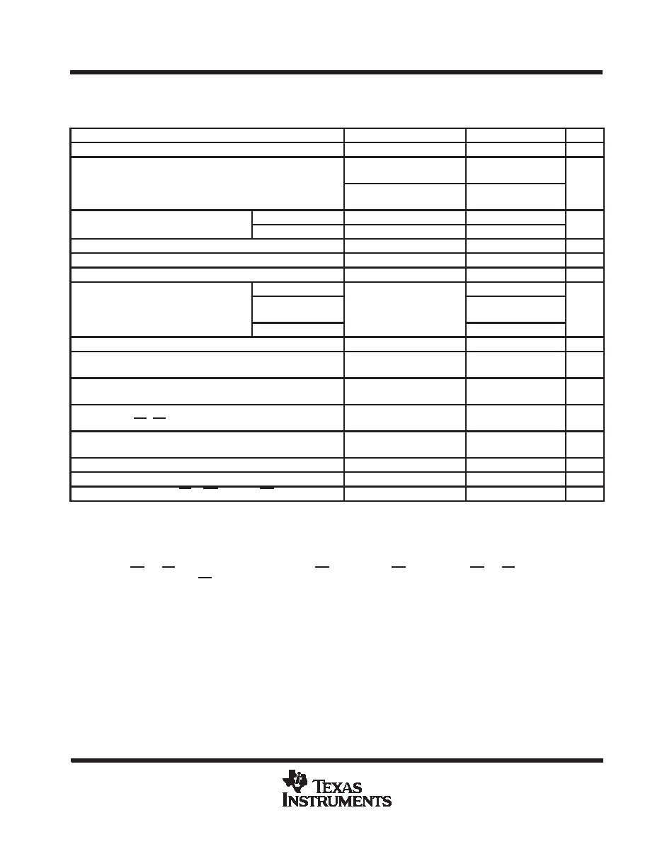
electrical characteristics over recommended operating free-air temperature range,
ANLG VCC+ = DGTL VCC = Vref = 5 V, ANLG VCC– = –5 V or ANLG GND, fclock = 2 MHz (unless
otherwise noted) (see Note 2)
PARAMETER
TEST CONDITIONS
MIN
TYP
MAX
UNIT
EL
Integral linearity error
±0.012%
FSR
– 5 V < (IN + – IN –) < 5 V,
≥ 1
1
§
ED
Differential linearity
()
,
VCC+ = 5 V, VCC – = – 5 V
≥–1
1
LSB§
ED
Differential linearity
0 < (IN + – IN –) < 5.05 V,
≥ 1
1
LSB§
()
,
VCC+ = 5 V, VCC – = 0
≥–1
1
Zero error
TLC1225I
±1.5
LSB
Zero error
TLC1225M
±1
LSB
Unadjusted positive and negative full-scale error
± 2
LSB
Temperature coefficient of gain
15
ppm/
°C
Temperature coefficient of offset point
1.5
ppm/
°C
Zero error
± 0.75
kSVS
Supply voltage sensitivity
Positive and negative
ANLG VCC + = 5 V ± 5%,
ANLG VCC
5V
±5%
± 075
LSB
kSVS
Supply voltage sensitivity
g
full-scale error
ANLG VCC – = – 5 V ± 5%,
DGTL VCC = 5V ± 5%
± 0.75
LSB
Linearity error
DGTL VCC = 5 V ± 5%
± 0.25
CMRR
Common-mode rejection ratio
IN – = IN + = – 5 V to 5 V
65
dB
Common-mode rejection (maximum code change
IN
=IN + =
5Vto5V
2
LSB
j(
g
from code 0000000000000)
IN – = IN + = – 5 V to 5 V
2
LSB
t
Conversion period (1/f lk) (see Notes 4 and 5)
f lk =26MHz
24
clock
tconv
Conversion period (1/fclock) (see Notes 4 and 5)
fclock = 2.6 MHz
24
cycles
t
Access time (delay from falling edge of
CL = 100 pF,
95
ns
ta
(y
g
CS
RD to data output)
L
,
fclock = 2.6 MHz
95
ns
tdi
Disable time, output (delay from rising edge of RD to
RL = 2 k,CL = 100 pF,
90
ns
tdis
,(
y
g
high-impedance state)
L
,
L
,
fclock = 2.6 MHz
90
ns
td1(READY)
Delay time, control signal edge to READY OUT
fclock = 2.6 MHz
100
ns
td2(READY)
Delay time, control signal edge to READY OUT
fclock = 2.6 MHz
100
ns
td(INT)
Delay time, RD or WR to reset of INT
fclock = 2.6 MHz
100
ns
All typical values are at TA = 25°C.
FSR is full-scale range: 0.012% FSR linearity error is equivalent to 1 LSB = 1.22 mV.
§ No missing codes
NOTES:
2. The input voltage range is defined as: VI+ = – 5.05 V to 5.05 V, VI– = – 5.05 V to 5.05 V, and | VI+ – VI– | ≤ 5.05 V when ANLG
VCC – = – 5 V. The input voltage range is defined as: VI+ = – 0.05 V to 5.05 V, VI– = – 0.05 V to 5.05 V, and | VI+ – VI– | ≤ 5.05 V when
ANLG VCC – = ANLG GND.
4. If INT and RD go low within the same fclock period, INT is not reset until WR is brought low. If INT and RD do not go low within the
same fclock period, INT is reset.
5. The conversion period is the reciprocal of the conversion rate and includes the access, sample, setup, and A/D conversion times.
相關(guān)PDF資料 |
PDF描述 |
|---|---|
| TLC1225IFN | 1-CH 12-BIT SUCCESSIVE APPROXIMATION ADC, PARALLEL ACCESS, PQCC28 |
| TLC1225MJ | 1-CH 12-BIT SUCCESSIVE APPROXIMATION ADC, PARALLEL ACCESS, CDIP28 |
| TLC1225IFNR | 1-CH 12-BIT SUCCESSIVE APPROXIMATION ADC, PARALLEL ACCESS, PQCC28 |
| TLC1514IPWLE | 4-CH 10-BIT SUCCESSIVE APPROXIMATION ADC, SERIAL ACCESS, PDSO16 |
| TLC1518IPWLE | 8-CH 10-BIT SUCCESSIVE APPROXIMATION ADC, SERIAL ACCESS, PDSO20 |
相關(guān)代理商/技術(shù)參數(shù) |
參數(shù)描述 |
|---|---|
| TLC1225MJB | 制造商:Rochester Electronics LLC 功能描述:- Bulk |
| TLC139 | 制造商:TI 制造商全稱:Texas Instruments 功能描述:LinCMOSE MICROPOWER QUAD COMPARATORS |
| TLC139D | 制造商:TI 制造商全稱:Texas Instruments 功能描述:LinCMOSE MICROPOWER QUAD COMPARATORS |
| TLC139FK | 制造商:TI 制造商全稱:Texas Instruments 功能描述:LinCMOSE MICROPOWER QUAD COMPARATORS |
| TLC139J | 制造商:TI 制造商全稱:Texas Instruments 功能描述:LinCMOSE MICROPOWER QUAD COMPARATORS |
發(fā)布緊急采購(gòu),3分鐘左右您將得到回復(fù)。