- 您現(xiàn)在的位置:買賣IC網(wǎng) > PDF目錄98234 > TLC1518IDWRG4 (TEXAS INSTRUMENTS INC) 8-CH 10-BIT SUCCESSIVE APPROXIMATION ADC, SERIAL ACCESS, PDSO20 PDF資料下載
參數(shù)資料
| 型號: | TLC1518IDWRG4 |
| 廠商: | TEXAS INSTRUMENTS INC |
| 元件分類: | ADC |
| 英文描述: | 8-CH 10-BIT SUCCESSIVE APPROXIMATION ADC, SERIAL ACCESS, PDSO20 |
| 封裝: | GREEN, PLASTIC, SOIC-20 |
| 文件頁數(shù): | 23/42頁 |
| 文件大小: | 645K |
| 代理商: | TLC1518IDWRG4 |
第1頁第2頁第3頁第4頁第5頁第6頁第7頁第8頁第9頁第10頁第11頁第12頁第13頁第14頁第15頁第16頁第17頁第18頁第19頁第20頁第21頁第22頁當(dāng)前第23頁第24頁第25頁第26頁第27頁第28頁第29頁第30頁第31頁第32頁第33頁第34頁第35頁第36頁第37頁第38頁第39頁第40頁第41頁第42頁
TLC1514, TLC1518
5-V, 10-BIT, 400 KSPS, 4/8 CHANNEL, LOW POWER,
SERIAL ANALOG-TO-DIGITAL CONVERTERS WITH AUTO POWER DOWN
SLAS252 – DECEMBER 1999
3
POST OFFICE BOX 655303
DALLAS, TEXAS 75265
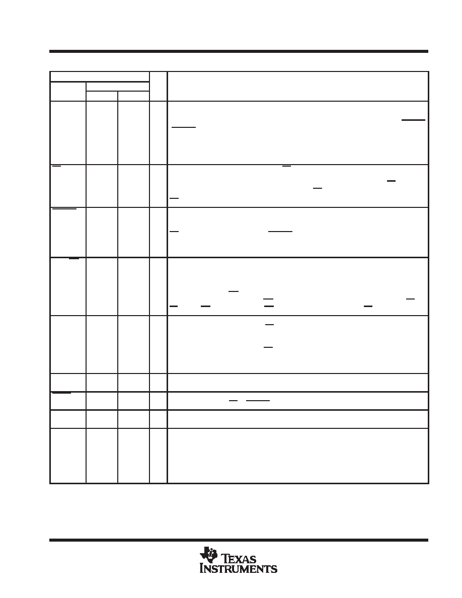
Terminal Functions
TERMINAL
NAME
NO.
I/O
DESCRIPTION
NAME
TLC1514
TLC1518
A0
A1
A2
A3
A4
A5
A6
A7
6
7
8
9
6
7
8
9
10
11
12
13
I
Analog signal inputs. The analog inputs are applied to these terminals and are internally
multiplexed. The driving source impedance should be less than or equal to 1 k
.
For a source impedance greater than 1 k
, use the asynchronous conversion start signal CSTART
(CSTART low time controls the sampling period) or program long sampling period to increase the
sampling time.
CS
16
20
I
Chip select. A high-to-low transition on the CS input resets the internal 4-bit counter, enables SDI,
and removes SDO from 3-state within a maximum setup time. SDI is disabled within a setup time
after the 4-bit counter counts to 16 (clock edges) or a low-to-high transition of CS whichever
happens first. SDO is 3-stated after the rising edge of CS.
CS can be used as the FS pin when a dedicated serial port is used.
CSTART
10
14
I
This terminal controls the start of sampling of the analog input from a selected multiplex channel.
A high-to-low transition starts sampling of the analog input signal. A low-to-high transition puts the
S/H in hold mode and starts the conversion. This input is independent from SCLK and works when
CS is high (inactive). The low time of CSTART controls the duration of the sampling period of the
converter (extended sampling).
Tie this terminal to VCC if not used.
EOC/(INT)
4
O
End of conversion or interrupt to host processor.
[PROGRAMMED AS EOC]: This output goes from a high-to-low logic level at the end of the
sampling period and remains low until the conversion is complete and data are ready for transfer.
EOC is used in conversion mode 00 only.
[PROGRAMMED AS INT]: This pin can also be programmed as an interrupt output signal to the
host processor. The falling edge of INT indicates data are ready for output. The following CS
↓ or
FS
↑ clears INT. The falling edge of INT puts SDO back to 3-state even if CS is still active.
FS
13
17
I
DSP frame sync input. Indication of the start of a serial data frame in or out of the device. If FS
remains low at the falling edge of CS, SDI is not enabled until an active FS is presented. A
high-to-low transition on the FS input resets the internal 4-bit counter and enables SDI within a
maximum setup time. SDI is disabled within a setup time after the 4-bit counter counts to 16 (clock
edges) or a low-to-high transition of CS whichever happens first. SDO is 3-stated after the 16th bit
is presented.
Tie this terminal to VCC if not used.
GND
11
15
I
Ground return for the internal circuitry. Unless otherwise noted, all voltage measurements are with
respect to GND.
PWDN
12
16
I
Both analog and reference circuits are powered down when this pin is at logic zero. The device can
be restarted by active CS or CSTART after this pin is pulled back to logic one.
SCLK
3
I
Input serial clock. This terminal receives the serial SCLK from the host processor. SCLK is used
to clock the input SDI to the input register. It is also used as the source of the conversion clock.
SDI
2
I
Serial data input. The input data is presented with the MSB (D15) first. The first 4-bit MSBs,
D(15–12) are decoded as one of the 16 commands (12 only for the TLC1514). All trailing blanks
are filled with zeros. The configure write commands require an additional 12 bits of data.
When FS is not used (FS =1), the first MSB (D15) is expected after the falling edge of CS and is
shifted in on the rising edges of SCLK (after CS
↓).
When FS is used (typical with an active FS from a DSP) the first MSB (D15) is expected after the
falling edge of FS and is shifted in on the falling edges of SCLK.
相關(guān)PDF資料 |
PDF描述 |
|---|---|
| TLC1514IDRG4 | 4-CH 10-BIT SUCCESSIVE APPROXIMATION ADC, SERIAL ACCESS, PDSO16 |
| TLC1518IDW | 8-CH 10-BIT SUCCESSIVE APPROXIMATION ADC, SERIAL ACCESS, PDSO20 |
| TLC1518IPWR | 8-CH 10-BIT SUCCESSIVE APPROXIMATION ADC, SERIAL ACCESS, PDSO20 |
| TLC1518IPWG4 | 8-CH 10-BIT SUCCESSIVE APPROXIMATION ADC, SERIAL ACCESS, PDSO20 |
| TLC1514ID | 4-CH 10-BIT SUCCESSIVE APPROXIMATION ADC, SERIAL ACCESS, PDSO16 |
相關(guān)代理商/技術(shù)參數(shù) |
參數(shù)描述 |
|---|---|
| TLC1518IPW | 功能描述:模數(shù)轉(zhuǎn)換器 - ADC 10bit 400kSPS SAR RoHS:否 制造商:Texas Instruments 通道數(shù)量:2 結(jié)構(gòu):Sigma-Delta 轉(zhuǎn)換速率:125 SPs to 8 KSPs 分辨率:24 bit 輸入類型:Differential 信噪比:107 dB 接口類型:SPI 工作電源電壓:1.7 V to 3.6 V, 2.7 V to 5.25 V 最大工作溫度:+ 85 C 安裝風(fēng)格:SMD/SMT 封裝 / 箱體:VQFN-32 |
| TLC1518IPWG4 | 功能描述:模數(shù)轉(zhuǎn)換器 - ADC 10-Bit 400 kSPS Serial Out RoHS:否 制造商:Texas Instruments 通道數(shù)量:2 結(jié)構(gòu):Sigma-Delta 轉(zhuǎn)換速率:125 SPs to 8 KSPs 分辨率:24 bit 輸入類型:Differential 信噪比:107 dB 接口類型:SPI 工作電源電壓:1.7 V to 3.6 V, 2.7 V to 5.25 V 最大工作溫度:+ 85 C 安裝風(fēng)格:SMD/SMT 封裝 / 箱體:VQFN-32 |
| TLC1518IPWR | 功能描述:模數(shù)轉(zhuǎn)換器 - ADC 10-Bit 400 kSPS Serial Out RoHS:否 制造商:Texas Instruments 通道數(shù)量:2 結(jié)構(gòu):Sigma-Delta 轉(zhuǎn)換速率:125 SPs to 8 KSPs 分辨率:24 bit 輸入類型:Differential 信噪比:107 dB 接口類型:SPI 工作電源電壓:1.7 V to 3.6 V, 2.7 V to 5.25 V 最大工作溫度:+ 85 C 安裝風(fēng)格:SMD/SMT 封裝 / 箱體:VQFN-32 |
| TLC1518IPWRG4 | 功能描述:模數(shù)轉(zhuǎn)換器 - ADC 10-Bit 400 kSPS Serial Out RoHS:否 制造商:Texas Instruments 通道數(shù)量:2 結(jié)構(gòu):Sigma-Delta 轉(zhuǎn)換速率:125 SPs to 8 KSPs 分辨率:24 bit 輸入類型:Differential 信噪比:107 dB 接口類型:SPI 工作電源電壓:1.7 V to 3.6 V, 2.7 V to 5.25 V 最大工作溫度:+ 85 C 安裝風(fēng)格:SMD/SMT 封裝 / 箱體:VQFN-32 |
| TLC1518PW | 制造商:TI 制造商全稱:Texas Instruments 功能描述:5-V, 10-BIT, 400 KSPS, 4/8 CHANNEL, LOW POWER, SERIAL ANALOG-TO-DIGITAL CONVERTERS WITH AUTO POWER DOWN |
發(fā)布緊急采購,3分鐘左右您將得到回復(fù)。