- 您現在的位置:買賣IC網 > PDF目錄98234 > TLC1541CDW (TEXAS INSTRUMENTS INC) 11-CH 10-BIT SUCCESSIVE APPROXIMATION ADC, SERIAL ACCESS, PDSO20 PDF資料下載
參數資料
| 型號: | TLC1541CDW |
| 廠商: | TEXAS INSTRUMENTS INC |
| 元件分類: | ADC |
| 英文描述: | 11-CH 10-BIT SUCCESSIVE APPROXIMATION ADC, SERIAL ACCESS, PDSO20 |
| 封裝: | GREEN, SOIC-20 |
| 文件頁數: | 7/13頁 |
| 文件大小: | 182K |
| 代理商: | TLC1541CDW |
TLC1541
10-BIT ANALOG-TO-DIGITAL CONVERTER
WITH SERIAL CONTROL AND 11 INPUTS
SLAS073C – DECEMBER 1995 – REVISED AUGUST 1996
3
POST OFFICE BOX 655303
DALLAS, TEXAS 75265
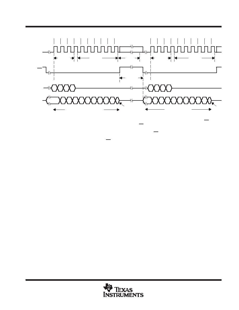
operating sequence
MSB
LSB
Don’t Care
MSB
LSB
twH(CS)
tconv
See Note A
See Note C
HI-Z
State
HI-Z State
Sample
Cycle C
Access
Cycle C
Sample
Cycle B
Access
Cycle B
Previous Conversion Data A
Conversion Data B
A9
B9
MSB
LSB MSB
MSB
LSB MSB
(see Note B)
B9
B8
B7
B6
B5 B4
B3
B2
B1
B0
A9
A8
A7
A6 A5
A4
A3
A2
A1
A0
B3
B2 B1
B0
C3
C2 C1
C0
Don’t
Care
1
2
3
4
56
7
8
9
10
1
2
3
4
56
7
8
9
10
I/O
CLOCK
ADDRESS
INPUT
DATA
OUT
CS
NOTES: A. The conversion cycle, which requires 44 system clock periods, initiates on the tenth falling edge of the I/O clock after CS goes low
for the channel whose address exists in memory at that time. When CS is kept low during conversion, the I/O clock must remain
low for at least 44 system clock cycles to allow the conversion to complete.
B. The most significant bit (MSB) is automatically placed on the DATA OUT bus after CS is brought low. The remaining nine bits (A8–A0)
clock out on the first nine I/O clock falling edges.
C. To minimize errors caused by noise at the CS input, the internal circuitry waits for three system clock cycles (or less) after a
chip-select falling edge is detected before responding to control input signals. Therefore, no attempt should be made to clock-in
address data until the minimum chip-select setup time elapses.
absolute maximum ratings over operating free-air temperature range (unless otherwise noted)
Supply voltage, VCC (see Note 1)
6.5 V
. . . . . . . . . . . . . . . . . . . . . . . . . . . . . . . . . . . . . . . . . . . . . . . . . . . . . . . . . . .
Input voltage range, VI (any input)
– 0.3 V to VCC + 0.3 V
. . . . . . . . . . . . . . . . . . . . . . . . . . . . . . . . . . . . . . . . . . . .
Output voltage range, VO
– 0.3 V to VCC + 0.3 V
. . . . . . . . . . . . . . . . . . . . . . . . . . . . . . . . . . . . . . . . . . . . . . . . . . .
Peak input current (any input)
±10 mA
. . . . . . . . . . . . . . . . . . . . . . . . . . . . . . . . . . . . . . . . . . . . . . . . . . . . . . . . . . . .
Peak total input current (all inputs)
±30 mA
. . . . . . . . . . . . . . . . . . . . . . . . . . . . . . . . . . . . . . . . . . . . . . . . . . . . . . . .
Operating free-air temperature range, TA: C suffix
0
°C to 70°C
. . . . . . . . . . . . . . . . . . . . . . . . . . . . . . . . . . . . . . .
I suffix
– 40
°C to 85°C
. . . . . . . . . . . . . . . . . . . . . . . . . . . . . . . . . . . . . .
Storage temperature range, Tstg
–65
°C to 150°C
. . . . . . . . . . . . . . . . . . . . . . . . . . . . . . . . . . . . . . . . . . . . . . . . . . .
Case temperature for 10 seconds, TC: FN package
260
°C
. . . . . . . . . . . . . . . . . . . . . . . . . . . . . . . . . . . . . . . . . .
Lead temperature 1,6 mm (1/16 inch) from the case for 10 seconds: DW or N package
260
°C
. . . . . . . . . . .
Stresses beyond those listed under “absolute maximum ratings” may cause permanent damage to the device. These are stress ratings only, and
functional operation of the device at these or any other conditions beyond those indicated under “recommended operating conditions” is not
implied. Exposure to absolute-maximum-rated conditions for extended periods may affect device reliability.
NOTE 1: All voltage values are with respect to digital ground with REF – and GND wired together (unless otherwise noted).
相關PDF資料 |
PDF描述 |
|---|---|
| TLC1541IDWR | 11-CH 10-BIT SUCCESSIVE APPROXIMATION ADC, SERIAL ACCESS, PDSO20 |
| TLC1541CDWG4 | 11-CH 10-BIT SUCCESSIVE APPROXIMATION ADC, SERIAL ACCESS, PDSO20 |
| TLC1541IDWG4 | 11-CH 10-BIT SUCCESSIVE APPROXIMATION ADC, SERIAL ACCESS, PDSO20 |
| TLC1541IDWRG4 | 11-CH 10-BIT SUCCESSIVE APPROXIMATION ADC, SERIAL ACCESS, PDSO20 |
| TLC1541IFNG3 | 11-CH 10-BIT SUCCESSIVE APPROXIMATION ADC, SERIAL ACCESS, PQCC20 |
相關代理商/技術參數 |
參數描述 |
|---|---|
| TLC1541CDWG4 | 功能描述:模數轉換器 - ADC 10-Bit 32 kSPS Serial Out RoHS:否 制造商:Texas Instruments 通道數量:2 結構:Sigma-Delta 轉換速率:125 SPs to 8 KSPs 分辨率:24 bit 輸入類型:Differential 信噪比:107 dB 接口類型:SPI 工作電源電壓:1.7 V to 3.6 V, 2.7 V to 5.25 V 最大工作溫度:+ 85 C 安裝風格:SMD/SMT 封裝 / 箱體:VQFN-32 |
| TLC1541CDWR | 功能描述:模數轉換器 - ADC 10-Bit 32 kSPS Serial Out RoHS:否 制造商:Texas Instruments 通道數量:2 結構:Sigma-Delta 轉換速率:125 SPs to 8 KSPs 分辨率:24 bit 輸入類型:Differential 信噪比:107 dB 接口類型:SPI 工作電源電壓:1.7 V to 3.6 V, 2.7 V to 5.25 V 最大工作溫度:+ 85 C 安裝風格:SMD/SMT 封裝 / 箱體:VQFN-32 |
| TLC1541CDWRG4 | 功能描述:模數轉換器 - ADC 10-Bit 32 kSPS Serial Out RoHS:否 制造商:Texas Instruments 通道數量:2 結構:Sigma-Delta 轉換速率:125 SPs to 8 KSPs 分辨率:24 bit 輸入類型:Differential 信噪比:107 dB 接口類型:SPI 工作電源電壓:1.7 V to 3.6 V, 2.7 V to 5.25 V 最大工作溫度:+ 85 C 安裝風格:SMD/SMT 封裝 / 箱體:VQFN-32 |
| TLC1541CFN | 功能描述:模數轉換器 - ADC 10bit 11Chl A/D RoHS:否 制造商:Texas Instruments 通道數量:2 結構:Sigma-Delta 轉換速率:125 SPs to 8 KSPs 分辨率:24 bit 輸入類型:Differential 信噪比:107 dB 接口類型:SPI 工作電源電壓:1.7 V to 3.6 V, 2.7 V to 5.25 V 最大工作溫度:+ 85 C 安裝風格:SMD/SMT 封裝 / 箱體:VQFN-32 |
| TLC1541CFNG3 | 功能描述:模數轉換器 - ADC 10-Bit 32 kSPS Serial Out RoHS:否 制造商:Texas Instruments 通道數量:2 結構:Sigma-Delta 轉換速率:125 SPs to 8 KSPs 分辨率:24 bit 輸入類型:Differential 信噪比:107 dB 接口類型:SPI 工作電源電壓:1.7 V to 3.6 V, 2.7 V to 5.25 V 最大工作溫度:+ 85 C 安裝風格:SMD/SMT 封裝 / 箱體:VQFN-32 |
發布緊急采購,3分鐘左右您將得到回復。