- 您現在的位置:買賣IC網 > PDF目錄98240 > TLC4545IDGKRG4 (TEXAS INSTRUMENTS INC) 1-CH 16-BIT SUCCESSIVE APPROXIMATION ADC, SERIAL ACCESS, PDSO8 PDF資料下載
參數資料
| 型號: | TLC4545IDGKRG4 |
| 廠商: | TEXAS INSTRUMENTS INC |
| 元件分類: | ADC |
| 英文描述: | 1-CH 16-BIT SUCCESSIVE APPROXIMATION ADC, SERIAL ACCESS, PDSO8 |
| 封裝: | GREEN, PLASTIC, MSOP-8 |
| 文件頁數: | 6/27頁 |
| 文件大小: | 666K |
| 代理商: | TLC4545IDGKRG4 |
第1頁第2頁第3頁第4頁第5頁當前第6頁第7頁第8頁第9頁第10頁第11頁第12頁第13頁第14頁第15頁第16頁第17頁第18頁第19頁第20頁第21頁第22頁第23頁第24頁第25頁第26頁第27頁
TLC4541, TLC4545
SLAS293 DECEMBER 2001
14
www.ti.com
PRINCIPLES OF OPERATION
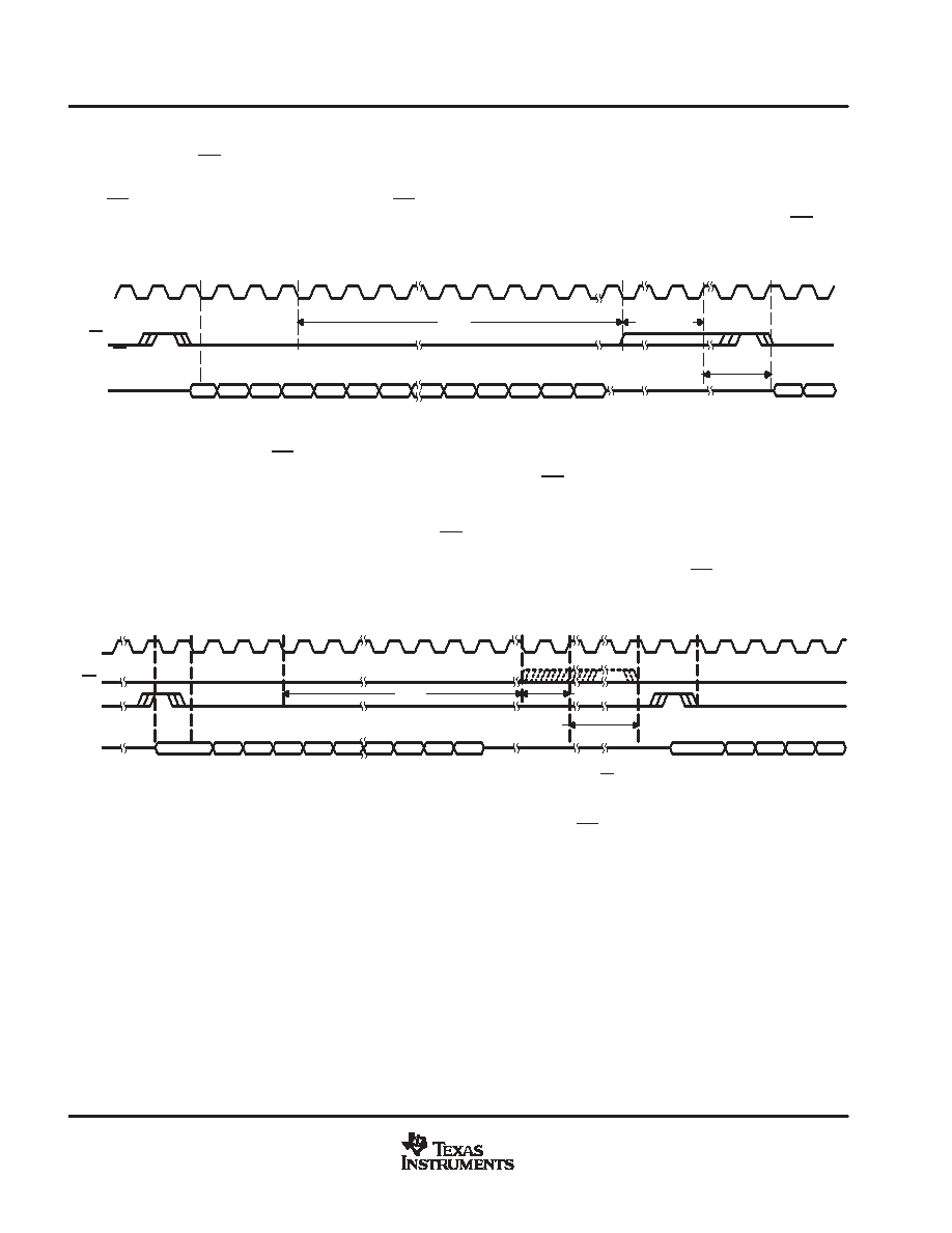
control via pin 1 (CS, DSP interface)
All devices are compatible with this mode of operation. The FS signal from a DSP is connected directly to the
CS input of the ADC. A falling edge on the CS input while SCLK is high or low initiates the cycle. (For TLC4541
in this configuration, the FS input is tied to VDD.) Enough time should be allowed before the next rising CS edge
so that the conversion cycle is not terminated prematurely.
1
2
3
5
4
6
7
13
14
15
16
1
12
ts
tconv
t(PWRDWN)
SDO Data is the Result of the Previous Sample
For TLC45xx, the LSB is Presented on the Rising SCLK 16th Edge
MSB
MSB1
MSB2 MSB3 MSB4 MSB5 MSB6
LSB4
LSB3
LSB2
LSB1
LSB
SCLK
CS
SDO
MSB
MSB1
The CS Input Signal is
Generated by the FS Output
From a TMS320 DSP
24
Figure 16. DSP Cycle Timing Using the CS Input (FS = 1 for TLC4541 Only)
control via pin 1 and pin 7 (CS and FS or FS only, DSP interface)
Only TLC4541 is compatible with this mode of operation. The CS input to the ADC can be controlled via a
general-purpose I/O pin from the DSP or tied to ground. The FS signal from the DSP is connected directly to
the FS input of the ADC. A rising FS edge releases the MSB to the SDO output. The falling edge on the FS input
while SCLK is high or low initiates the cycle. The CS input should remain low for the entire sampling time plus
4 SCLK decoding time after falling FS (24 falling SCLK edges) and can then be released at any time during the
remainder of the conversion cycle. The optimum DSP interface is achieved when tying CS to ground and using
only the FS input to control the ADC.
tconv
t(PWRDWN)
SDO Data is the Result of the Previous Sample
For TLC45xx, the LSB is Presented on the Rising SCLK 16th Edge
1
2
3
5
4
6
14
15
16
1
2
34
ts
MSB
MSB1 MSB2 MSB3 MSB4 MSB5 LSB3
LSB2 LSB1
LSB
MSB
MSB1 MSB2 MSB3
The MSB is Presented on the SDO Output After
a Rising Edge on the FS Input.
17
24
The Device Will go into the Power Down State After the Conversion is
Complete. A Falling CS Edge or Rising FS Edge, Whichever Occurs First,
Removes the Device From Power Down.
SCLK
CS
SDO
FS
Figure 17. DSP Cycle Timing Using FS Only (or Using Both CS and FS for the TLC4541)
相關PDF資料 |
PDF描述 |
|---|---|
| TLC4541IDRG4 | 1-CH 16-BIT SUCCESSIVE APPROXIMATION ADC, SERIAL ACCESS, PDSO8 |
| TLC540INSG4 | 11-CH 8-BIT SUCCESSIVE APPROXIMATION ADC, SERIAL ACCESS, PDSO20 |
| TLC540INS | 11-CH 8-BIT SUCCESSIVE APPROXIMATION ADC, SERIAL ACCESS, PDSO20 |
| TLC541INSG4 | 11-CH 8-BIT SUCCESSIVE APPROXIMATION ADC, SERIAL ACCESS, PDSO20 |
| TLC541INS | 11-CH 8-BIT SUCCESSIVE APPROXIMATION ADC, SERIAL ACCESS, PDSO20 |
相關代理商/技術參數 |
參數描述 |
|---|---|
| TLC4545IDR | 功能描述:模數轉換器 - ADC 16-Bit 200KSPS Serial Out RoHS:否 制造商:Texas Instruments 通道數量:2 結構:Sigma-Delta 轉換速率:125 SPs to 8 KSPs 分辨率:24 bit 輸入類型:Differential 信噪比:107 dB 接口類型:SPI 工作電源電壓:1.7 V to 3.6 V, 2.7 V to 5.25 V 最大工作溫度:+ 85 C 安裝風格:SMD/SMT 封裝 / 箱體:VQFN-32 |
| TLC4545IDRG4 | 功能描述:模數轉換器 - ADC 16-Bit 200KSPS Serial Out RoHS:否 制造商:Texas Instruments 通道數量:2 結構:Sigma-Delta 轉換速率:125 SPs to 8 KSPs 分辨率:24 bit 輸入類型:Differential 信噪比:107 dB 接口類型:SPI 工作電源電壓:1.7 V to 3.6 V, 2.7 V to 5.25 V 最大工作溫度:+ 85 C 安裝風格:SMD/SMT 封裝 / 箱體:VQFN-32 |
| TLC-4C-0375 | 制造商:KATO/COILTHREAD 功能描述: |
| TLC-4C-0375W | 制造商:KATO/COILTHREAD 功能描述: |
| TLC-4C-0500 | 制造商:KATO/COILTHREAD 功能描述: |
發布緊急采購,3分鐘左右您將得到回復。