- 您現在的位置:買賣IC網 > PDF目錄98240 > TLC542IFNG3 (TEXAS INSTRUMENTS INC) 11-CH 8-BIT SUCCESSIVE APPROXIMATION ADC, SERIAL ACCESS, PQCC20 PDF資料下載
參數資料
| 型號: | TLC542IFNG3 |
| 廠商: | TEXAS INSTRUMENTS INC |
| 元件分類: | ADC |
| 英文描述: | 11-CH 8-BIT SUCCESSIVE APPROXIMATION ADC, SERIAL ACCESS, PQCC20 |
| 封裝: | GREEN, PLASTIC, LCC-20 |
| 文件頁數: | 7/12頁 |
| 文件大小: | 172K |
| 代理商: | TLC542IFNG3 |
TLC542C, TLC542I
8-BIT ANALOG-TO-DIGITAL CONVERTERS
WITH SERIAL CONTROL AND 11 INPUTS
SLAS075C – FEBRUARY 1989 – REVISED JUNE 2001
4
POST OFFICE BOX 655303
DALLAS, TEXAS 75265
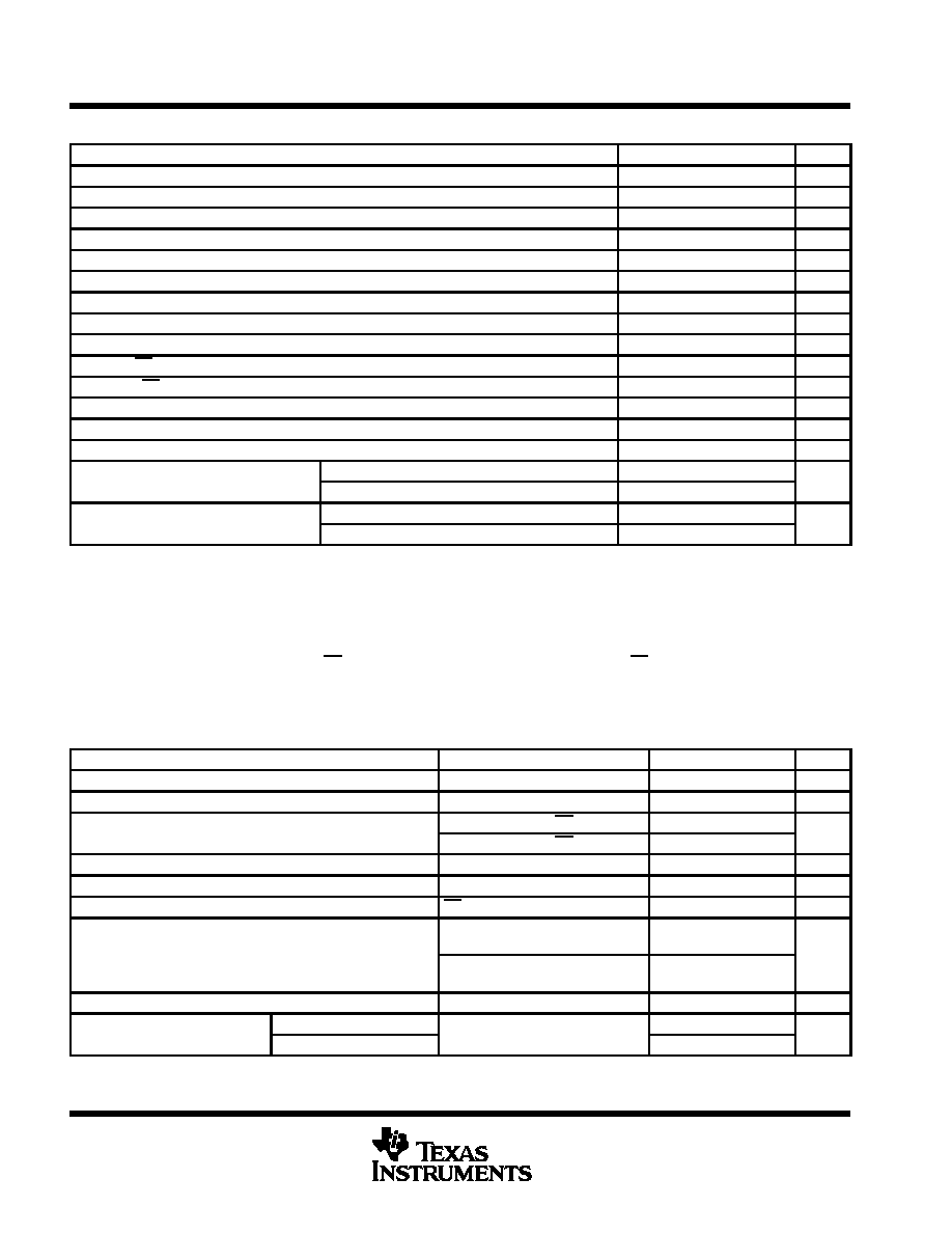
recommended operating conditions, VCC = 4.75 to 5.5 V
MIN
NOM
MAX
UNIT
Supply voltage, VCC
4.75
5
5.5
V
Positive reference voltage, Vref + (see Note 2)
Vref–
VCC
VCC + 0.1
V
Negative reference voltage, Vref – (see Note 2)
– 0.1
0
Vref+
V
Differential reference voltage, Vref+ – Vref– (see Note 2)
1
VCC
VCC + 0.2
V
Analog input voltage (see Note 3)
0
VCC
V
High-level control input voltage, VIH
2
V
Low-level control input voltage, VIL
0.8
V
Setup time, address bits at data input before I/O CLOCK
↑, tsu(A)
400
ns
Hold time, address bits after I/O CLOCK
↑, th(A)
0
ns
Hold time, CS low after 8th I/O CLOCK
↑, th(CS)
0
ns
Setup time, CS low before clocking in first address bit, tsu(CS) (see Note 4)
3.8
s
Input/output clock frequency, f(clock I/O)
0
1.1
MHz
Input/output clock high, tw(H I/O)
404
ns
Input/output clock low, tw(L I/O)
404
ns
I/O CLOCK transition time tt (see Note 3)
fclock(I/O) ≤ 525 kHz
100
ns
I/O CLOCK transition time, tt (see Note 3)
fclock(I/O) > 525 kHz
40
ns
Operating free air temperature TA
TLC542C
0
70
°C
Operating free-air temperature, TA
TLC542I
– 40
85
°C
NOTES:
2. Analog input voltages greater than that applied to REF+ convert as all ones (11111111), while input voltages less than that applied
to REF – convert as all zeros (00000000). For proper operation, REF+ must be at least 1 V higher than REF –. Also, the total
unadjusted error may increase as this differential reference voltage falls below 4.75 V.
3. This is the time required for the clock input signal to fall from VIH min to VIL max or to rise from VIL max to VIH min. In the vicinity
of normal room temperature, the devices function with input clock transition time as slow as 2
s for remote data acquisition
applications where the sensor and the A/D converter are placed several feet away from the controlling microprocessor.
4. To minimize errors caused by noise at the chip select input, the internal circuitry waits for two rising edges and one falling edge of
the internal system clock after CS
↓ before responding to control input signals. The CS setup time is given by the tsu(CS)
specifications. Therefore, no attempt should be made to clock-in address data until the minimum chip select setup time has elapsed.
electrical characteristics over recommended operating temperature range, VCC = Vref+ = 4.75 V to
5.5 V, f(clock I/O) = 1.1 MHz (unless otherwise noted)
PARAMETER
TEST CONDITIONS
MIN
TYP
MAX
UNIT
VOH
High-level output voltage (DATA OUT)
VCC = 4.75 V,
IOH = – 360 A
2.4
V
VOL
Low-level output voltage
VCC = 4.75 V,
IOL = 1.6 mA
0.4
V
Off state (high impedance state) output current
VO = VCC,
CS at VCC
10
A
Off-state (high-impedance state) output current
VO = 0,
CS at VCC
–10
A
IIH
High-level input current
VI = VCC
0.005
2
A
IIL
Low-level input current
VI = 0
– 0.005
– 2.5
A
ICC
Operating supply current
CS at 0 V
1.2
2
mA
Selected channel leakage current
Selected channel at VCC and
unselected channel at 0 V
0.4
A
Selected channel leakage current
Selected channel at 0 V and
unselected channel at VCC
– 0.4
A
Iref
Maximum static analog reference current into REF+
Vref+ = VCC,
Vref – = GND
10
A
Ci
Input capacitance
Analog inputs
7
55
pF
Ci
Input capacitance
Control inputs
5
15
pF
All typical values are at TA = 25°C.
相關PDF資料 |
PDF描述 |
|---|---|
| TLC542CDWRG4 | 11-CH 8-BIT SUCCESSIVE APPROXIMATION ADC, SERIAL ACCESS, PDSO20 |
| TLC542IN | 11-CH 8-BIT SUCCESSIVE APPROXIMATION ADC, SERIAL ACCESS, PDIP20 |
| TLC542IDW | 11-CH 8-BIT SUCCESSIVE APPROXIMATION ADC, SERIAL ACCESS, PDSO20 |
| TLC542CN | 11-CH 8-BIT SUCCESSIVE APPROXIMATION ADC, SERIAL ACCESS, PDIP20 |
| TLC542CDWR | 11-CH 8-BIT SUCCESSIVE APPROXIMATION ADC, SERIAL ACCESS, PDSO20 |
相關代理商/技術參數 |
參數描述 |
|---|---|
| TLC542IFNR | 功能描述:模數轉換器 - ADC 8bit 25ksps 11ch 5V RoHS:否 制造商:Texas Instruments 通道數量:2 結構:Sigma-Delta 轉換速率:125 SPs to 8 KSPs 分辨率:24 bit 輸入類型:Differential 信噪比:107 dB 接口類型:SPI 工作電源電壓:1.7 V to 3.6 V, 2.7 V to 5.25 V 最大工作溫度:+ 85 C 安裝風格:SMD/SMT 封裝 / 箱體:VQFN-32 |
| TLC542IFNRG3 | 功能描述:模數轉換器 - ADC 8-Bit 25 kSPS Serial-Out RoHS:否 制造商:Texas Instruments 通道數量:2 結構:Sigma-Delta 轉換速率:125 SPs to 8 KSPs 分辨率:24 bit 輸入類型:Differential 信噪比:107 dB 接口類型:SPI 工作電源電壓:1.7 V to 3.6 V, 2.7 V to 5.25 V 最大工作溫度:+ 85 C 安裝風格:SMD/SMT 封裝 / 箱體:VQFN-32 |
| TLC542IN | 功能描述:模數轉換器 - ADC 8bit A/D w/Osc RoHS:否 制造商:Texas Instruments 通道數量:2 結構:Sigma-Delta 轉換速率:125 SPs to 8 KSPs 分辨率:24 bit 輸入類型:Differential 信噪比:107 dB 接口類型:SPI 工作電源電壓:1.7 V to 3.6 V, 2.7 V to 5.25 V 最大工作溫度:+ 85 C 安裝風格:SMD/SMT 封裝 / 箱體:VQFN-32 |
| TLC542INE4 | 功能描述:模數轉換器 - ADC 8-Bit 25 kSPS Serial-Out RoHS:否 制造商:Texas Instruments 通道數量:2 結構:Sigma-Delta 轉換速率:125 SPs to 8 KSPs 分辨率:24 bit 輸入類型:Differential 信噪比:107 dB 接口類型:SPI 工作電源電壓:1.7 V to 3.6 V, 2.7 V to 5.25 V 最大工作溫度:+ 85 C 安裝風格:SMD/SMT 封裝 / 箱體:VQFN-32 |
| TLC545 | 制造商:TI 制造商全稱:Texas Instruments 功能描述:8-BIT ANALOG-TO-DIGITAL CONVERTERS WITH SERIAL CONTROL AND 19 INPUTS |
發布緊急采購,3分鐘左右您將得到回復。