- 您現在的位置:買賣IC網 > PDF目錄98242 > TLC5510IPW (TEXAS INSTRUMENTS INC) 1-CH 8-BIT FLASH METHOD ADC, PARALLEL ACCESS, PDSO24 PDF資料下載
參數資料
| 型號: | TLC5510IPW |
| 廠商: | TEXAS INSTRUMENTS INC |
| 元件分類: | ADC |
| 英文描述: | 1-CH 8-BIT FLASH METHOD ADC, PARALLEL ACCESS, PDSO24 |
| 封裝: | GREEN, PLASTIC, TSSOP-24 |
| 文件頁數: | 18/21頁 |
| 文件大小: | 500K |
| 代理商: | TLC5510IPW |
TLC5510, TLC5510A
8-BIT HIGH-SPEED ANALOG-TO-DIGITAL CONVERTERS
SLAS095L – SEPTEMBER 1994 – REVISED JUNE 2003
6
POST OFFICE BOX 655303
DALLAS, TEXAS 75265
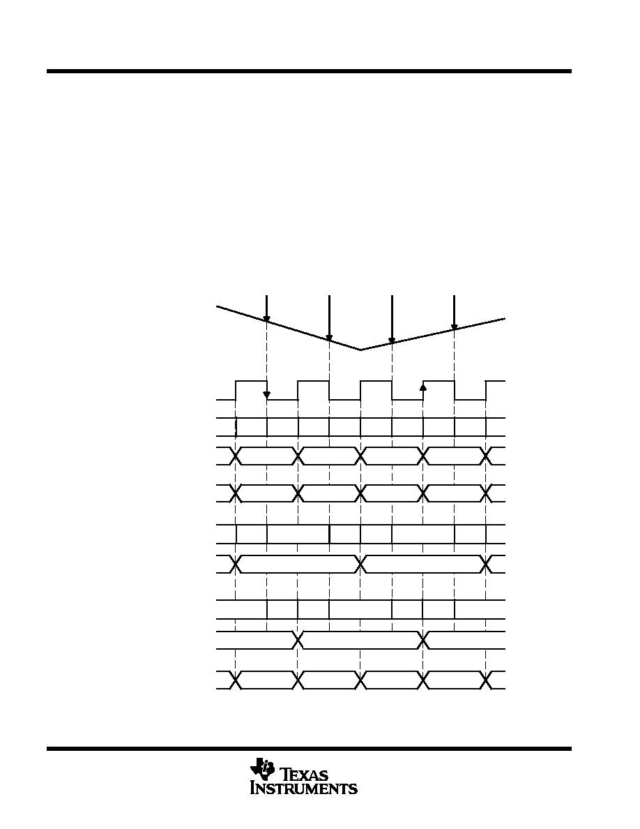
PRINCIPLES OF OPERATION
functional description
The TLC5510 and TLC5510A are semiflash ADCs featuring two lower comparator blocks of four bits each.
As shown in Figure 2, input voltage VI(1) is sampled with the falling edge of CLK1 to the upper comparators block
and the lower comparators block(A), S(1). The upper comparators block finalizes the upper data UD(1) with the
rising edge of CLK2, and simultaneously, the lower reference voltage generates the voltage RV(1)
corresponding to the upper data. The lower comparators block (A) finalizes the lower data LD(1) with the rising
edge of CLK3. UD(1) and LD(1) are combined and output as OUT(1) with the rising edge of CLK4. As shown
in Figure 2, the output data is delayed 2.5 clocks from the analog input voltage sampling point.
Input voltage VI(2) is sampled with the falling edge of CLK2. UD(2) is finalized with the rising edge of CLK3, and
LD(2) is finalized with the rising edge of CLK4 at the lower comparators block(B). OUT(2) data appears with
the rising edge of CLK5.
VI(1)
VI(2)
VI(3)
VI(4)
CLK1
CLK2
CLK3
CLK4
S(1)
C(1)
S(2)
C(2)
S(3)
C(3)
S(4)
C(4)
S(1)
H(1)
C(1)
S(3)
H(3)
C(3)
H(0)
C(0)
S(2)
H(2)
C(2)
S(4)
H(4)
LD(– 2)
OUT(– 2)
OUT(–1)
OUT(0)
OUT(1)
ANALOG IN
(sampling points)
CLK (clock)
Upper Comparators Block
Upper Data
Lower Reference Voltage
Lower Comparators Block (A)
Lower Data (A)
Lower Comparators Block (B)
Lower Data (B)
D1 – D8 (data output)
UD(0)
RV(0)
UD(1)
RV(1)
UD(2)
RV(2)
UD(3)
RV(3)
LD(– 1)
LD(0)
LD(1)
LD(2)
CLK5
Figure 2. Internal Functional Timing Diagram
相關PDF資料 |
PDF描述 |
|---|---|
| TLC5510AINS | 1-CH 8-BIT FLASH METHOD ADC, PARALLEL ACCESS, PDSO24 |
| TLC5510IANSLE | 1-CH 8-BIT FLASH METHOD ADC, SERIAL ACCESS, PDSO24 |
| TLC5510INSG4 | 1-CH 8-BIT FLASH METHOD ADC, PARALLEL ACCESS, PDSO24 |
| TLC5510INS | 1-CH 8-BIT FLASH METHOD ADC, PARALLEL ACCESS, PDSO24 |
| TLC551CDBLE | PULSE; RECTANGULAR, 1.2 MHz, TIMER, PDSO8 |
相關代理商/技術參數 |
參數描述 |
|---|---|
| TLC5510IPWG4 | 功能描述:視頻模擬/數字化轉換器集成電路 8-Bit 20 MSPS 1-Ch Internal S&H Lo Pwr RoHS:否 制造商:Texas Instruments 輸入信號類型:Differential 轉換器數量:1 ADC 輸入端數量:4 轉換速率:3 Gbps 分辨率:8 bit 結構: 輸入電壓:3.3 V 接口類型:SPI 信噪比: 電壓參考: 電源電壓-最大:3.45 V 電源電壓-最小:3.15 V 最大功率耗散: 最大工作溫度:+ 85 C 最小工作溫度:- 40 C 封裝 / 箱體:TCSP-48 封裝:Reel |
| TLC5510IPWR | 功能描述:模數轉換器 - ADC 8-Bit 20 MSPS 1-Ch Internal S&H Lo Pwr RoHS:否 制造商:Texas Instruments 通道數量:2 結構:Sigma-Delta 轉換速率:125 SPs to 8 KSPs 分辨率:24 bit 輸入類型:Differential 信噪比:107 dB 接口類型:SPI 工作電源電壓:1.7 V to 3.6 V, 2.7 V to 5.25 V 最大工作溫度:+ 85 C 安裝風格:SMD/SMT 封裝 / 箱體:VQFN-32 |
| TLC5510IPWRG4 | 功能描述:視頻模擬/數字化轉換器集成電路 8-Bit 20 MSPS 1-Ch Internal S&H Lo Pwr RoHS:否 制造商:Texas Instruments 輸入信號類型:Differential 轉換器數量:1 ADC 輸入端數量:4 轉換速率:3 Gbps 分辨率:8 bit 結構: 輸入電壓:3.3 V 接口類型:SPI 信噪比: 電壓參考: 電源電壓-最大:3.45 V 電源電壓-最小:3.15 V 最大功率耗散: 最大工作溫度:+ 85 C 最小工作溫度:- 40 C 封裝 / 箱體:TCSP-48 封裝:Reel |
| TLC551CD | 功能描述:計時器和支持產品 CMOS RoHS:否 制造商:Micrel 類型:Standard 封裝 / 箱體:SOT-23 內部定時器數量:1 電源電壓-最大:18 V 電源電壓-最小:2.7 V 最大功率耗散: 最大工作溫度:+ 85 C 最小工作溫度:- 40 C 封裝:Reel |
| TLC551CDBLE | 制造商:TI 制造商全稱:Texas Instruments 功能描述:LinCMOSE TIMERS |
發布緊急采購,3分鐘左右您將得到回復。