- 您現在的位置:買賣IC網 > PDF目錄98242 > TLC5540CPWRG4 (TEXAS INSTRUMENTS INC) 1-CH 8-BIT FLASH METHOD ADC, PARALLEL ACCESS, PDSO24 PDF資料下載
參數資料
| 型號: | TLC5540CPWRG4 |
| 廠商: | TEXAS INSTRUMENTS INC |
| 元件分類: | ADC |
| 英文描述: | 1-CH 8-BIT FLASH METHOD ADC, PARALLEL ACCESS, PDSO24 |
| 封裝: | GREEN, PLASTIC, TSSOP-24 |
| 文件頁數: | 3/21頁 |
| 文件大小: | 407K |
| 代理商: | TLC5540CPWRG4 |
TLC5540
SLAS105D JANUARY 1995 REVISED APRIL 2004
www.ti.com
11
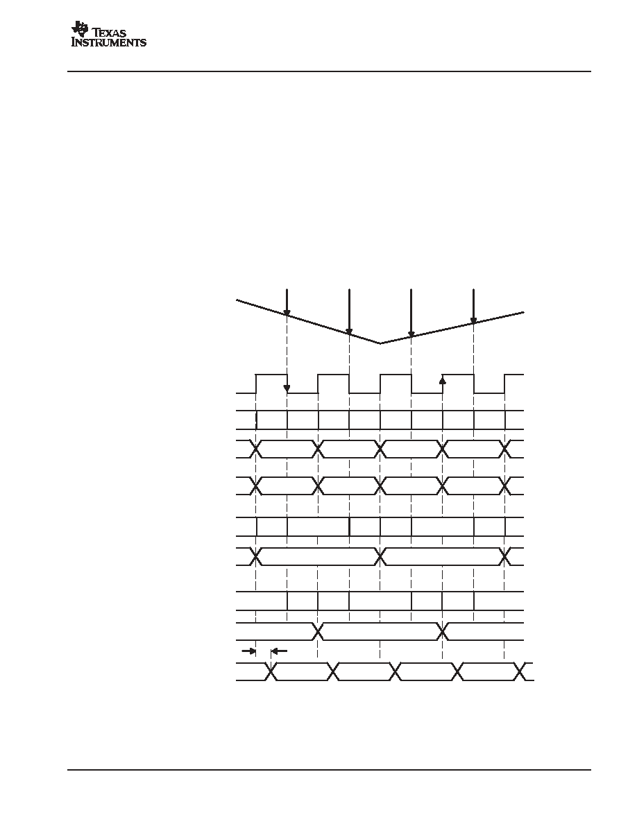
PRINCIPLES OF OPERATION
functional description
The TLC5540 uses a modified semiflash architecture as shown in the functional block diagram. The four most
significant bits (MSBs) of every output conversion result are produced by the upper comparator block CB1. The
four least significant bits (LSBs) of each alternate output conversion result are produced by the lower
comparator blocks CB-A and CB-B in turn (see Figure 12).
The reference voltage that is applied to the lower comparator resistor string is one sixteenth of the amplitude
of the refence applied to the upper comparator resistor string. The sampling comparators of the lower
comparator block require more time to sample the lower voltages of the reference and residual input voltage.
By applying the residual input voltage to alternate lower comparator blocks, each comparator block has twice
as much time to sample and convert as would be the case if only one lower comparator block were used.
VI(1)
VI(2)
VI(3)
VI(4)
CLK1
CLK2
CLK3
CLK4
S(1)
C(1)
S(2)
C(2)
S(3)
C(3)
S(4)
C(4)
S(1)
H(1)
C(1)
S(3)
H(3)
C(3)
H(0)
C(0)
S(2)
H(2)
C(2)
S(4)
H(4)
LD(2)
OUT(2)
OUT(1)
OUT(0)
OUT(1)
ANALOG IN
(Sampling Points)
CLK (Clock)
Upper Comparators Block (CB1)
Upper Data
Lower Reference Voltage
Lower Comparators Block (CB-A)
Lower Data (A)
Lower Comparators Block (CB-B)
Lower Data (B)
D1 D8 (Data Output)
UD(0)
RV(0)
UD(1)
RV(1)
UD(2)
RV(2)
UD(3)
RV(3)
LD(1)
LD(0)
LD(1)
LD(2)
tpd
Figure 12. Internal Functional Timing Diagram
This conversion scheme, which reduces the required sampling comparators by 30 percent compared to
standard semiflash architectures, achieves significantly higher sample rates than the conventional semiflash
conversion method.
相關PDF資料 |
PDF描述 |
|---|---|
| TLC5540IPWR | 1-CH 8-BIT FLASH METHOD ADC, PARALLEL ACCESS, PDSO24 |
| TLC5540IPWG4 | 1-CH 8-BIT FLASH METHOD ADC, PARALLEL ACCESS, PDSO24 |
| TLC5540CPW | 1-CH 8-BIT FLASH METHOD ADC, PARALLEL ACCESS, PDSO24 |
| TLC5540CPWG4 | 1-CH 8-BIT FLASH METHOD ADC, PARALLEL ACCESS, PDSO24 |
| TLC5540INSLE | 1-CH 8-BIT FLASH METHOD ADC, PARALLEL ACCESS, PDSO24 |
相關代理商/技術參數 |
參數描述 |
|---|---|
| TLC5540EVM | 功能描述:數據轉換 IC 開發工具 TLC5540 Eval Mod RoHS:否 制造商:Texas Instruments 產品:Demonstration Kits 類型:ADC 工具用于評估:ADS130E08 接口類型:SPI 工作電源電壓:- 6 V to + 6 V |
| TLC5540INS | 功能描述:模數轉換器 - ADC 8B,40MSPS ADC Sgl Ch Internal S&H,Lo Pwr RoHS:否 制造商:Texas Instruments 通道數量:2 結構:Sigma-Delta 轉換速率:125 SPs to 8 KSPs 分辨率:24 bit 輸入類型:Differential 信噪比:107 dB 接口類型:SPI 工作電源電壓:1.7 V to 3.6 V, 2.7 V to 5.25 V 最大工作溫度:+ 85 C 安裝風格:SMD/SMT 封裝 / 箱體:VQFN-32 |
| TLC5540INS | 制造商:Texas Instruments 功能描述:IC 8BIT ADC SMD 5540 SOIC24 |
| TLC5540INSG4 | 功能描述:模數轉換器 - ADC 8B,40 MSPS ADC RoHS:否 制造商:Texas Instruments 通道數量:2 結構:Sigma-Delta 轉換速率:125 SPs to 8 KSPs 分辨率:24 bit 輸入類型:Differential 信噪比:107 dB 接口類型:SPI 工作電源電壓:1.7 V to 3.6 V, 2.7 V to 5.25 V 最大工作溫度:+ 85 C 安裝風格:SMD/SMT 封裝 / 箱體:VQFN-32 |
| TLC5540INSLE | 制造商:TI 制造商全稱:Texas Instruments 功能描述:8-BIT HIGH-SPEED ANALOG-TO-DIGITAL CONVERTER |
發布緊急采購,3分鐘左右您將得到回復。