- 您現在的位置:買賣IC網 > PDF目錄98243 > TLC5615IP (TEXAS INSTRUMENTS INC) SERIAL INPUT LOADING, 12.5 us SETTLING TIME, 10-BIT DAC, PDIP8 PDF資料下載
參數資料
| 型號: | TLC5615IP |
| 廠商: | TEXAS INSTRUMENTS INC |
| 元件分類: | DAC |
| 英文描述: | SERIAL INPUT LOADING, 12.5 us SETTLING TIME, 10-BIT DAC, PDIP8 |
| 封裝: | ROHS COMPLIANT, PLASTIC, DIP-8 |
| 文件頁數: | 3/22頁 |
| 文件大小: | 552K |
| 代理商: | TLC5615IP |
www.ti.com
DAC Code
Output
Voltage
0 V
Negative
Offset
POWER-SUPPLY BYPASSING AND GROUND MANAGEMENT
0.1
F
Analog Ground Plane
1
2
3
4
8
7
6
5
SAVING POWER
SLAS142E – OCTOBER 1996 – REVISED JUNE 2007
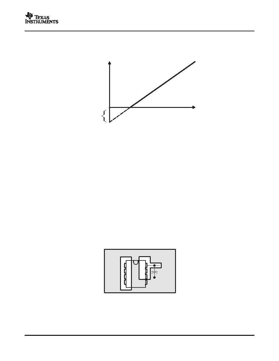
The output amplifier attempts to drive the output to a negative voltage. However, because the most negative
supply rail is ground, the output cannot drive below ground and clamps the output at 0V.
The output voltage then remains at zero until the input code value produces a sufficient positive output voltage
to overcome the negative offset voltage, resulting in the transfer function shown in Figure 14.
Figure 14. Effect of Negative Offset (Single Supply)
This offset error, not the linearity error, produces this breakpoint. The transfer function would have followed the
dotted line if the output buffer could drive below the ground rail.
For a DAC, linearity is measured between zero-input code (all inputs '0') and full-scale code (all inputs '1') after
offset and full scale are adjusted out or accounted for in some way. However, single supply operation does not
allow for adjustment when the offset is negative due to the breakpoint in the transfer function. So the linearity is
measured between full-scale code and the lowest code that produces a positive output voltage. For the
TLC5615, the zero-scale (offset) error is
±3LSB maximum. The code is calculated from the maximum
specification for the negative offset.
Printed circuit boards that use separate analog and digital ground planes offer the best system performance.
Wire-wrap boards do not perform well and should not be used. The two ground planes should be connected
together at the low-impedance power-supply source. The best ground connection may be achieved by
connecting the DAC AGND terminal to the system analog ground plane making sure that analog ground currents
are well managed and there are negligible voltage drops across the ground plane.
A 0.1
F ceramic-capacitor bypass should be connected between V
DD and AGND and mounted with short leads
as close as possible to the device. Use of ferrite beads may further isolate the system analog supply from the
digital power supply.
Figure 15 shows the ground plane layout and bypassing technique.
Figure 15. Power-Supply Bypassing
Setting the DAC register to all 0s minimizes power consumption by the reference resistor array and the output
load when the system is not using the DAC.
11
相關PDF資料 |
PDF描述 |
|---|---|
| TLC5615CDR | SERIAL INPUT LOADING, 12.5 us SETTLING TIME, 10-BIT DAC, PDSO8 |
| TLC5615CDG4 | SERIAL INPUT LOADING, 12.5 us SETTLING TIME, 10-BIT DAC, PDSO8 |
| TLC5615IPE4 | SERIAL INPUT LOADING, 12.5 us SETTLING TIME, 10-BIT DAC, PDIP8 |
| TLC5615IDGKR | SERIAL INPUT LOADING, 12.5 us SETTLING TIME, 10-BIT DAC, PDSO8 |
| TLC5615CPE4 | SERIAL INPUT LOADING, 12.5 us SETTLING TIME, 10-BIT DAC, PDIP8 |
相關代理商/技術參數 |
參數描述 |
|---|---|
| TLC5615IPE4 | 功能描述:數模轉換器- DAC 10-Bit 12.5 us DAC Serial Input Lo-Pwr RoHS:否 制造商:Texas Instruments 轉換器數量:1 DAC 輸出端數量:1 轉換速率:2 MSPs 分辨率:16 bit 接口類型:QSPI, SPI, Serial (3-Wire, Microwire) 穩定時間:1 us 最大工作溫度:+ 85 C 安裝風格:SMD/SMT 封裝 / 箱體:SOIC-14 封裝:Tube |
| TLC5617 | 制造商:TI 制造商全稱:Texas Instruments 功能描述:PROGRAMMABLE DUAL 10-BIT DIGITAL-TO-ANALOG CONVERTERS |
| TLC5617A | 制造商:TI 制造商全稱:Texas Instruments 功能描述:PROGRAMMABLE DUAL 10-BIT DIGITAL-TO-ANALOG CONVERTERS |
| TLC5617A1D | 制造商:Rochester Electronics LLC 功能描述:- Bulk 制造商:Texas Instruments 功能描述: |
| TLC5617ACD | 制造商:Rochester Electronics LLC 功能描述:- Bulk 制造商:Texas Instruments 功能描述: |
發布緊急采購,3分鐘左右您將得到回復。