- 您現在的位置:買賣IC網 > PDF目錄98243 > TLC5628IDWR (TEXAS INSTRUMENTS INC) OCTAL, SERIAL INPUT LOADING, 10 us SETTLING TIME, 8-BIT DAC, PDSO16 PDF資料下載
參數資料
| 型號: | TLC5628IDWR |
| 廠商: | TEXAS INSTRUMENTS INC |
| 元件分類: | DAC |
| 英文描述: | OCTAL, SERIAL INPUT LOADING, 10 us SETTLING TIME, 8-BIT DAC, PDSO16 |
| 文件頁數: | 11/17頁 |
| 文件大小: | 407K |
| 代理商: | TLC5628IDWR |
TLC5628C, TLC5628I
OCTAL 8-BIT DIGITAL-TO-ANALOG CONVERTERS
SLAS089E – NOVEMBER 1994 – REVISED APRIL 1997
3
POST OFFICE BOX 655303
DALLAS, TEXAS 75265
detailed description
The TLC5628 is implemented using eight resistor-string DACs. The core of each DAC is a single resistor with
256 taps, corresponding to the 256 possible codes listed in Table 1. One end of each resistor string is connected
to GND and the other end is fed from the output of the reference input buffer. Monotonicity is maintained by use
of the resistor strings. Linearity depends upon the matching of the resistor segments and upon the performance
of the output buffer. Since the inputs are buffered, the DACs always present a high-impedance load to the
reference sources. There are two input reference terminals; REF1 is used for DACA through DACD and REF2
is used by DACE through DACH.
Each DAC output is buffered by a configurable-gain output amplifier, that can be programmed to times 1 or times
2 gain.
On power up, the DACs are reset to CODE 0.
Each output voltage is given by:
V
O
(DACA|B|C|D|E|F|G|H)
+ REF
CODE
256
(1
) RNG bit value)
where CODE is in the range 0 to 255 and the range (RNG) bit is a 0 or 1 within the serial control word.
Table 1. Ideal Output Transfer
D7
D6
D5
D4
D3
D2
D1
D0
OUTPUT VOLTAGE
0
GND
0
0000001
(1/256)
× REF (1+RNG)
0
1111111
(127/256)
× REF (1+RNG)
1
0000000
(128/256)
× REF (1+RNG)
1
(255/256)
× REF (1+RNG)
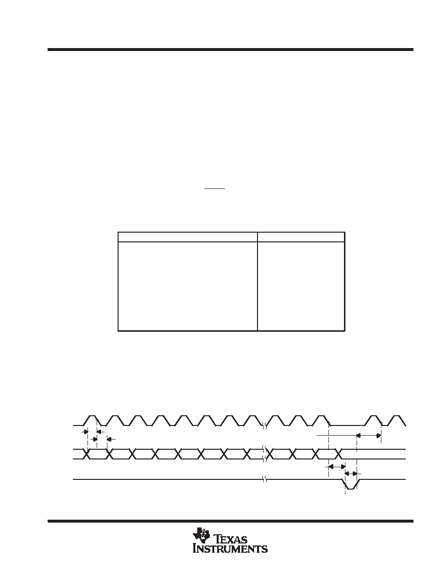
data interface
With LOAD high, data is clocked into the DATA terminal on each falling edge of CLK. Once all data bits have
been clocked in, LOAD is pulsed low to transfer the data from the serial input register to the selected DAC as
shown in Figure 1. When LDAC is low, the selected DAC output voltage is updated when LOAD goes low. When
LDAC is high during serial programming, the new value is stored within the device and can be transferred to
the DAC output at a later time by pulsing LDAC low as shown in Figure 2. Data is entered most significant bit
(MSB) first. Data transfers using two 8-clock cycle periods are shown in Figures 3 and 4.
A2
A1
A0
RNG
D7
D6
D5
D4
D2
D1
D0
DAC Update
CLK
DATA
LOAD
tsu(DATA-CLK)
tv(DATA-CLK)
tsu(CLK-LOAD)
tw(LOAD)
tsu(LOAD-CLK)
Figure 1. LOAD-Controlled Update (LDAC = Low)
相關PDF資料 |
PDF描述 |
|---|---|
| TLC5628IDWRG4 | OCTAL, SERIAL INPUT LOADING, 10 us SETTLING TIME, 8-BIT DAC, PDSO16 |
| TLC5628CDWRG4 | OCTAL, SERIAL INPUT LOADING, 10 us SETTLING TIME, 8-BIT DAC, PDSO16 |
| TLC5628CN | OCTAL, SERIAL INPUT LOADING, 10 us SETTLING TIME, 8-BIT DAC, PDIP16 |
| TLC5628IDWLE | OCTAL, SERIAL INPUT LOADING, 10 us SETTLING TIME, 8-BIT DAC, PDSO16 |
| TLC5628CDWLE | OCTAL, SERIAL INPUT LOADING, 10 us SETTLING TIME, 8-BIT DAC, PDSO16 |
相關代理商/技術參數 |
參數描述 |
|---|---|
| TLC5628IDWRG4 | 功能描述:數模轉換器- DAC 8Bit 10us Octal DAC Serial In Pgrmable RoHS:否 制造商:Texas Instruments 轉換器數量:1 DAC 輸出端數量:1 轉換速率:2 MSPs 分辨率:16 bit 接口類型:QSPI, SPI, Serial (3-Wire, Microwire) 穩定時間:1 us 最大工作溫度:+ 85 C 安裝風格:SMD/SMT 封裝 / 箱體:SOIC-14 封裝:Tube |
| TLC5628IN | 功能描述:數模轉換器- DAC Octal 8bit D/A RoHS:否 制造商:Texas Instruments 轉換器數量:1 DAC 輸出端數量:1 轉換速率:2 MSPs 分辨率:16 bit 接口類型:QSPI, SPI, Serial (3-Wire, Microwire) 穩定時間:1 us 最大工作溫度:+ 85 C 安裝風格:SMD/SMT 封裝 / 箱體:SOIC-14 封裝:Tube |
| TLC5628INE4 | 功能描述:數模轉換器- DAC 8Bit 10us Octal DAC Serial In Pgrmable RoHS:否 制造商:Texas Instruments 轉換器數量:1 DAC 輸出端數量:1 轉換速率:2 MSPs 分辨率:16 bit 接口類型:QSPI, SPI, Serial (3-Wire, Microwire) 穩定時間:1 us 最大工作溫度:+ 85 C 安裝風格:SMD/SMT 封裝 / 箱體:SOIC-14 封裝:Tube |
| TLC5733 | 制造商:TI 制造商全稱:Texas Instruments 功能描述:20 MSPS 3-CHANNEL ANALOG-TO-DIGITAL CONVERTER |
| TLC5733A | 制造商:TI 制造商全稱:Texas Instruments 功能描述:20 MSPS 3-CHANNEL ANALOG-TO-DIGITAL CONVERTER WITH HIGH-PRECISION CLAMP |
發布緊急采購,3分鐘左右您將得到回復。