- 您現在的位置:買賣IC網 > PDF目錄98245 > TLC7528EPWR (TEXAS INSTRUMENTS INC) DUAL, PARALLEL, 8 BITS INPUT LOADING, 0.1 us SETTLING TIME, 8-BIT DAC, PDSO20 PDF資料下載
參數資料
| 型號: | TLC7528EPWR |
| 廠商: | TEXAS INSTRUMENTS INC |
| 元件分類: | DAC |
| 英文描述: | DUAL, PARALLEL, 8 BITS INPUT LOADING, 0.1 us SETTLING TIME, 8-BIT DAC, PDSO20 |
| 封裝: | TSSOP-20 |
| 文件頁數: | 22/26頁 |
| 文件大小: | 616K |
| 代理商: | TLC7528EPWR |
TLC7528C, TLC7528E, TLC7528I
DUAL 8-BIT MULTIPLYING
DIGITAL-TO-ANALOG CONVERTERS
SLAS062C – JANUARY 1987 – REVISED SEPTEMBER 2000
5
POST OFFICE BOX 655303
DALLAS, TEXAS 75265
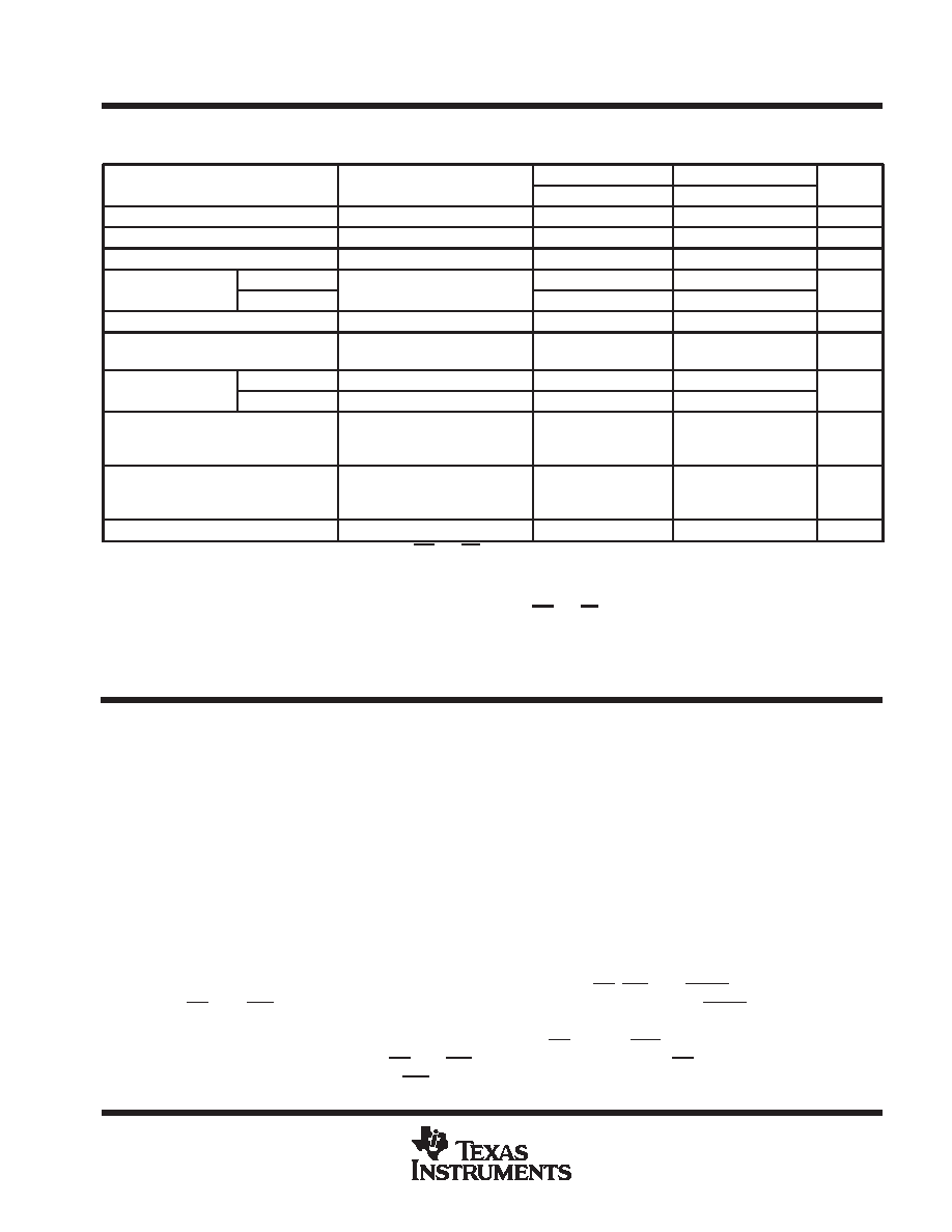
operating characteristics over recommended operating free-air temperature range,
VrefA = VrefB = 10 V, VOA and VOB at 0 V (unless otherwise noted)
PARAMETER
TEST CONDITIONS
VDD = 5 V
VDD = 15 V
UNIT
PARAMETER
TEST CONDITIONS
MIN
TYP
MAX
MIN
TYP
MAX
UNIT
Linearity error
±1/2
LSB
Settling time (to 1/2 LSB)
See Note 1
100
ns
Gain error
See Note 2
2.5
LSB
AC feedthrough
REFA to OUTA
See Note 3
–65
dB
AC feedthrough
REFB to OUTB
See Note 3
–65
dB
Temperature coefficient of gain
See Note 4
0.007
0.0035
%FSR/
°C
Propagation delay (from digital input to
90% of final analog output current)
See Note 5
80
ns
Channel-to-channel
REFA to OUTB
See Note 6
77
dB
isolation
REFB to OUTA
See Note 7
77
dB
Digital-to-analog glitch impulse area
Measured for code transition
from 00000000 to 11111111,
TA = 25°C
160
440
nV
s
Digital crosstalk
Measured for code transition
from 00000000 to 11111111,
TA = 25°C
30
60
nV
s
Harmonic distortion
Vi = 6 V, f = 1 kHz, TA = 25°C
–85
dB
NOTES:
1. OUTA, OUTB load = 100
, Cext = 13 pF; WR and CS at 0 V; DB0–DB7 at 0 V to VDD or VDD to 0 V.
2. Gain error is measured using an internal feedback resistor. Nominal full scale range (FSR) = Vref – 1 LSB.
3. Vref = 20 V peak-to-peak, 100-kHz sine wave; DAC data latches loaded with 00000000.
4. Temperature coefficient of gain measured from 0
°C to 25°C or from 25°C to 70°C.
5. VrefA = VrefB = 10 V; OUTA/OUTB load = 100 , Cext = 13 pF; WR and CS at 0 V; DB0–DB7 at 0 V to VDD or VDD to 0 V.
6. Both DAC latches loaded with 11111111; VrefA = 20 V peak-to-peak, 100-kHz sine wave; VrefB = 0; TA = 25°C.
7. Both DAC latches loaded with 11111111; VrefB = 20 V peak-to-peak, 100-kHz sine wave; VrefA = 0; TA = 25°C.
PRINCIPLES OF OPERATION
These devices contain two identical, 8-bit-multiplying D/A converters, DACA and DACB. Each DAC consists
of an inverted R-2R ladder, analog switches, and input data latches. Binary-weighted currents are switched
between DAC output and AGND, thus maintaining a constant current in each ladder leg independent of the
switch state. Most applications require only the addition of an external operational amplifier and voltage
reference. A simplified D/A circuit for DACA with all digital inputs low is shown in Figure 1.
Figure 2 shows the DACA equivalent circuit. A similar equivalent circuit can be drawn for DACB. Both DACs
share the analog ground terminal 1 (AGND). With all digital inputs high, the entire reference current flows to
OUTA. A small leakage current (IIkg) flows across internal junctions, and as with most semiconductor devices,
doubles every 10
°C. Co is due to the parallel combination of the NMOS switches and has a value that depends
on the number of switches connected to the output. The range of Co is 50 pF to 120 pF maximum. The equivalent
output resistance (ro) varies with the input code from 0.8R to 3R where R is the nominal value of the ladder
resistor in the R-2R network.
These devices interface to a microprocessor through the data bus, CS, WR, and DACA/DACB control signals.
When CS and WR are both low, the TLC7528 analog output, specified by the DACA/DACB control line,
responds to the activity on the DB0–DB7 data bus inputs. In this mode, the input latches are transparent and
input data directly affects the analog output. When either the CS signal or WR signal goes high, the data on the
DB0–DB7 inputs is latched until the CS and WR signals go low again. When CS is high, the data inputs are
disabled regardless of the state of the WR signal.
相關PDF資料 |
PDF描述 |
|---|---|
| TLC7528EFNR | DUAL, PARALLEL, 8 BITS INPUT LOADING, 0.1 us SETTLING TIME, 8-BIT DAC, PQCC20 |
| TLC7528EPW | DUAL, PARALLEL, 8 BITS INPUT LOADING, 0.1 us SETTLING TIME, 8-BIT DAC, PDSO20 |
| TLC7528IFNRG3 | PARALLEL, 8 BITS INPUT LOADING, 0.1 us SETTLING TIME, 8-BIT DAC, PQCC20 |
| TLC7628IN | PARALLEL, 8 BITS INPUT LOADING, 0.1 us SETTLING TIME, 8-BIT DAC, PDIP20 |
| TLC7628CDWR | PARALLEL, 8 BITS INPUT LOADING, 0.1 us SETTLING TIME, 8-BIT DAC, PDSO20 |
相關代理商/技術參數 |
參數描述 |
|---|---|
| TLC7528I | 制造商:TI 制造商全稱:Texas Instruments 功能描述:DUAL 8-BIT MULTIPLYING DIGITAL-TO-ANALOG CONVERTERS |
| TLC7528IDW | 功能描述:數模轉換器- DAC Dual 8bit Mult RoHS:否 制造商:Texas Instruments 轉換器數量:1 DAC 輸出端數量:1 轉換速率:2 MSPs 分辨率:16 bit 接口類型:QSPI, SPI, Serial (3-Wire, Microwire) 穩定時間:1 us 最大工作溫度:+ 85 C 安裝風格:SMD/SMT 封裝 / 箱體:SOIC-14 封裝:Tube |
| TLC7528IDWG4 | 功能描述:數模轉換器- DAC 8-Bit 0.1 us Dual MDAC RoHS:否 制造商:Texas Instruments 轉換器數量:1 DAC 輸出端數量:1 轉換速率:2 MSPs 分辨率:16 bit 接口類型:QSPI, SPI, Serial (3-Wire, Microwire) 穩定時間:1 us 最大工作溫度:+ 85 C 安裝風格:SMD/SMT 封裝 / 箱體:SOIC-14 封裝:Tube |
| TLC7528IDWR | 功能描述:數模轉換器- DAC 8-Bit 0.1 us Dual MDAC RoHS:否 制造商:Texas Instruments 轉換器數量:1 DAC 輸出端數量:1 轉換速率:2 MSPs 分辨率:16 bit 接口類型:QSPI, SPI, Serial (3-Wire, Microwire) 穩定時間:1 us 最大工作溫度:+ 85 C 安裝風格:SMD/SMT 封裝 / 箱體:SOIC-14 封裝:Tube |
| TLC7528IDWRG4 | 功能描述:數模轉換器- DAC 8-Bit 0.1 us Dual MDAC RoHS:否 制造商:Texas Instruments 轉換器數量:1 DAC 輸出端數量:1 轉換速率:2 MSPs 分辨率:16 bit 接口類型:QSPI, SPI, Serial (3-Wire, Microwire) 穩定時間:1 us 最大工作溫度:+ 85 C 安裝風格:SMD/SMT 封裝 / 箱體:SOIC-14 封裝:Tube |
發布緊急采購,3分鐘左右您將得到回復。