- 您現在的位置:買賣IC網 > PDF目錄98246 > TLE2426MDREP (TEXAS INSTRUMENTS INC) SPECIALTY ANALOG CIRCUIT, PDSO8 PDF資料下載
參數資料
| 型號: | TLE2426MDREP |
| 廠商: | TEXAS INSTRUMENTS INC |
| 元件分類: | 模擬信號調理 |
| 英文描述: | SPECIALTY ANALOG CIRCUIT, PDSO8 |
| 封裝: | PLASTIC, MS-012AA, SOIC-8 |
| 文件頁數: | 1/16頁 |
| 文件大小: | 431K |
| 代理商: | TLE2426MDREP |
TLE2426EP
RAIL SPLITTER
PRECISION VIRTUAL GROUND
SGLS345 JUNE 2006
1
POST OFFICE BOX 655303
DALLAS, TEXAS 75265
D Controlled Baseline
One Assembly/Test Site, One Fabrication
Site
D Extended Temperature Performance of
55
°C to 125°C
D Enhanced Diminishing Manufacturing
Sources (DMS) Support
D Enhanced Product-Change Notification
D Qualification Pedigree
D One-Half VI Virtual Ground for Analog
Systems
D Micropower Operation . . . 170 A Typ,
VI = 5 V
D Wide VI Range ...4 V to 40 V
D High Output-Current Capability
Source . . . 20 mA Typ
Sink . . . 20 mA Typ
D Excellent Output Regulation
102
V Typ at IO = 0 mA to 10 mA
49
V Typ at IO = 0 mA to 10 mA
D Low-Impedance Output . . . 0.0075 Typ
D Noise Reduction Pin
Component qualification in accordance with JEDEC and industry
standards to ensure reliable operation over an extended
temperature range. This includes, but is not limited to, Highly
Accelerated Stress Test (HAST) or biased 85/85, temperature
cycle, autoclave or unbiased HAST, electromigration, bond
intermetallic life, and mold compound life. Such qualification
testing should not be viewed as justifying use of this component
beyond specified performance and environmental limits.
description/ordering information
In signal-conditioning applications utilizing a
single power source, a reference voltage equal to
one-half the supply voltage is required for
termination of all analog signal grounds. TI
presents a precision virtual ground whose output
voltage is always equal to one-half the input
voltage—the TLE2426 rail splitter.
The unique combination of a high-performance,
micropower operational amplifier and a precision-
trimmed divider on a single silicon chip results in
a precise VO/VI ratio of 0.5 while sinking and
sourcing current. The TLE2426 provides a low-
impedance output with 20 mA of sink and source
capability, while drawing less than 280
A of
supply current over the full input range of 4 V to
40 V. A designer need not pay the price in terms
of board space for a conventional signal ground
consisting of resistors, capacitors, operational
amplifiers, and voltage references. For increased
performance, the 8-pin package provides a
noise-reduction pin. With the addition of an
external capacitor (CNR), peak-to-peak noise is
reduced, while line ripple rejection is improved.
Initial output tolerance for a single 5-V or 12-V system is better than 1% over the full 40-V input range. Ripple
rejection exceeds 12 bits of accuracy. Whether the application is for a data-acquisition front end, analog signal
termination, or simply a precision voltage reference, the TLE2426 eliminates a major source of system error.
Copyright
2006 Texas Instruments Incorporated
PRODUCTION DATA information is current as of publication date.
Products conform to specifications per the terms of Texas Instruments
standard warranty. Production processing does not necessarily include
testing of all parameters.
Please be aware that an important notice concerning availability, standard warranty, and use in critical applications of
Texas Instruments semiconductor products and disclaimers thereto appears at the end of this data sheet.
1
2
3
4
8
7
6
5
OUT
COMMON
IN
NC
NOISE REDUCTION
NC
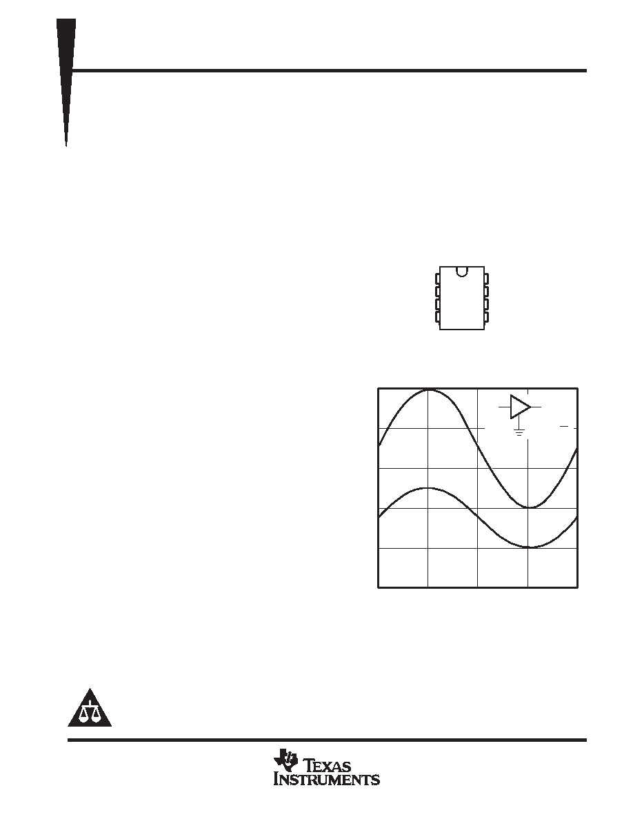
D PACKAGE
(TOP VIEW)
NC No internal connection
VO
VI
4
2
0
8
6
0
0.25
0.5
0.75
1
V
o
ltage
V
INPUT/OUTPUT TRANSFER CHARACTERISTICS
10
V
O +
V
I
2
VI
VO
t Time s
相關PDF資料 |
PDF描述 |
|---|---|
| TLE4202B | BRUSH DC MOTOR CONTROLLER, 2.5 A, PZFM7 |
| TLE4203S | BRUSH DC MOTOR CONTROLLER, 6 A, PSFM7 |
| TLE4209A | BRUSH DC MOTOR CONTROLLER, PDIP8 |
| TLE4251G | 1-CHANNEL POWER SUPPLY SUPPORT CKT, PSSO5 |
| TLE4726G | STEPPER MOTOR CONTROLLER, 1 A, PDSO24 |
相關代理商/技術參數 |
參數描述 |
|---|---|
| TLE2426MJGB | 制造商:Rochester Electronics LLC 功能描述:- Bulk 制造商:Texas Instruments 功能描述: |
| TLE2426QDRG4Q1 | 功能描述:基準電壓& 基準電流 AC Rail Splitter RoHS:否 制造商:STMicroelectronics 產品:Voltage References 拓撲結構:Shunt References 參考類型:Programmable 輸出電壓:1.24 V to 18 V 初始準確度:0.25 % 平均溫度系數(典型值):100 PPM / C 串聯 VREF - 輸入電壓(最大值): 串聯 VREF - 輸入電壓(最小值): 分流電流(最大值):60 mA 最大工作溫度:+ 125 C 封裝 / 箱體:SOT-23-3L 封裝:Reel |
| TLE2426QDRQ1 | 功能描述:基準電壓& 基準電流 AC Rail Splitter RoHS:否 制造商:STMicroelectronics 產品:Voltage References 拓撲結構:Shunt References 參考類型:Programmable 輸出電壓:1.24 V to 18 V 初始準確度:0.25 % 平均溫度系數(典型值):100 PPM / C 串聯 VREF - 輸入電壓(最大值): 串聯 VREF - 輸入電壓(最小值): 分流電流(最大值):60 mA 最大工作溫度:+ 125 C 封裝 / 箱體:SOT-23-3L 封裝:Reel |
| TLE26621DWR | 制造商:Rochester Electronics LLC 功能描述:- Bulk 制造商:Texas Instruments 功能描述: |
| TLE2662IDW | 制造商:Rochester Electronics LLC 功能描述:- Bulk |
發布緊急采購,3分鐘左右您將得到回復。