- 您現在的位置:買賣IC網 > PDF目錄98249 > TLV1549CD (TEXAS INSTRUMENTS INC) 1-CH 10-BIT SUCCESSIVE APPROXIMATION ADC, SERIAL ACCESS, PDSO8 PDF資料下載
參數資料
| 型號: | TLV1549CD |
| 廠商: | TEXAS INSTRUMENTS INC |
| 元件分類: | ADC |
| 英文描述: | 1-CH 10-BIT SUCCESSIVE APPROXIMATION ADC, SERIAL ACCESS, PDSO8 |
| 封裝: | GREEN, SOIC-8 |
| 文件頁數: | 16/19頁 |
| 文件大小: | 429K |
| 代理商: | TLV1549CD |
TLV1549C, TLV1549I, TLV1549M
10-BIT ANALOG-TO-DIGITAL CONVERTERS
WITH SERIAL CONTROL
SLAS071C – JANUARY 1993 – REVISED MARCH 1995
6
POST OFFICE BOX 655303
DALLAS, TEXAS 75265
SC
Threshold
Detector
NODE 512
REF –
REF+
ST
512
VI
To Output
Latches
1
2
4
8
16
128
256
REF+
REF –
ST
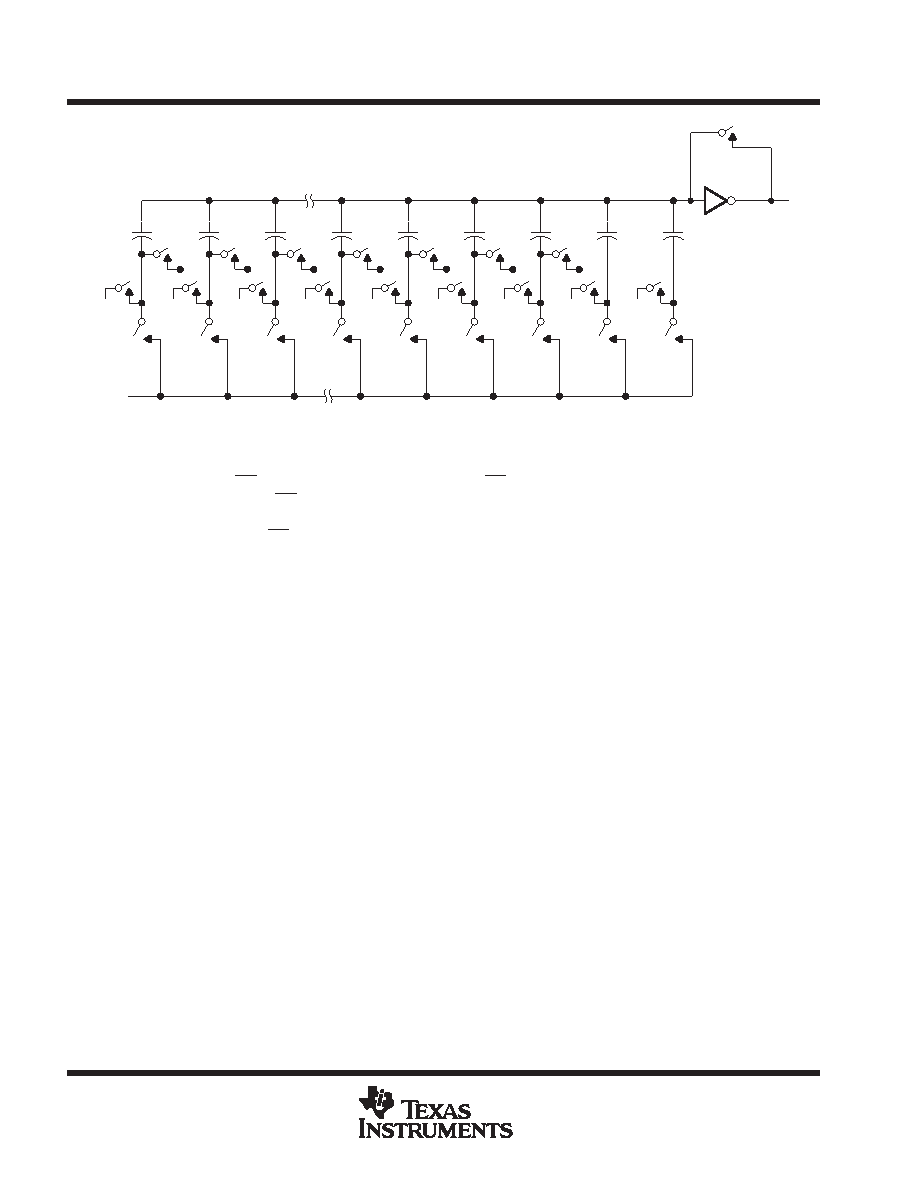
Figure 1. Simplified Model of the Successive-Approximation System
chip-select operation
The trailing edge of CS starts all modes of operation, and CS can abort a conversion sequence in any mode.
A high-to-low transition on CS within the specified time during an ongoing cycle aborts the cycle, and the device
returns to the initial state (the contents of the output data register remain at the previous conversion result).
Exercise care to prevent CS from being taken low close to completion of conversion because the output data
may be corrupted.
reference voltage inputs
There are two reference inputs used with the TLV1549: REF+ and REF–. These voltage values establish the
upper and lower limits of the analog input to produce a full-scale and zero reading, respectively. The values of
REF+, REF–, and the analog input should not exceed the positive supply or be lower than GND consistent with
the specified absolute maximum ratings. The digital output is at full scale when the input signal is equal to or
higher than REF+ and at zero when the input signal is equal to or lower than REF–.
absolute maximum ratings over operating free-air temperature range (unless otherwise noted)
Supply voltage range, VCC (see Note 1): TLV1549C
–0.5 V to 6.5 V
. . . . . . . . . . . . . . . . . . . . . . . . . . . . . . . . . .
TLV1549I
–0.5 V to 6.5 V
. . . . . . . . . . . . . . . . . . . . . . . . . . . . . . . . . . .
TLV1549M
–0.5 V to 6 V
. . . . . . . . . . . . . . . . . . . . . . . . . . . . . . . . . . .
Input voltage range, VI (any input)
–0.3 V to VCC + 0.3 V
. . . . . . . . . . . . . . . . . . . . . . . . . . . . . . . . . . . . . . . . . . . .
Output voltage range, VO
–0.3 V to VCC + 0.3 V
. . . . . . . . . . . . . . . . . . . . . . . . . . . . . . . . . . . . . . . . . . . . . . . . . . .
Positive reference voltage, Vref+
VCC + 0.1 V
. . . . . . . . . . . . . . . . . . . . . . . . . . . . . . . . . . . . . . . . . . . . . . . . . . . . . .
Negative reference voltage, Vref–
–0.1 V
. . . . . . . . . . . . . . . . . . . . . . . . . . . . . . . . . . . . . . . . . . . . . . . . . . . . . . . . . .
Peak input current (any input)
±20 mA
. . . . . . . . . . . . . . . . . . . . . . . . . . . . . . . . . . . . . . . . . . . . . . . . . . . . . . . . . . . .
Peak total input current (all inputs)
±30 mA
. . . . . . . . . . . . . . . . . . . . . . . . . . . . . . . . . . . . . . . . . . . . . . . . . . . . . . . .
Operating free-air temperature range, TA: TLV1549C
0
°C to 70°C
. . . . . . . . . . . . . . . . . . . . . . . . . . . . . . . . . . .
TLV1549I
–40
°C to 85°C
. . . . . . . . . . . . . . . . . . . . . . . . . . . . . . . . . .
TLV1549M
–55
°C to 125°C
. . . . . . . . . . . . . . . . . . . . . . . . . . . . . . . .
Storage temperature range, Tstg
–65
°C to 150°C
. . . . . . . . . . . . . . . . . . . . . . . . . . . . . . . . . . . . . . . . . . . . . . . . . . .
Lead temperature 1,6 mm (1/16 inch) from the case for 10 seconds
260
°C
. . . . . . . . . . . . . . . . . . . . . . . . . . . .
Stresses beyond those listed under “absolute maximum ratings” may cause permanent damage to the device. These are stress ratings only, and
functional operation of the device at these or any other conditions beyond those indicated under “recommended operating conditions” is not
implied. Exposure to absolute-maximum-rated conditions for extended periods may affect device reliability.
NOTE 1: All voltage values are with respect to ground with REF – and GND wired together (unless otherwise noted).
相關PDF資料 |
PDF描述 |
|---|---|
| TLV1562CDWRG4 | 4-CH 10-BIT PROPRIETARY METHOD ADC, PARALLEL ACCESS, PDSO28 |
| TLV1562CDWG4 | 4-CH 10-BIT PROPRIETARY METHOD ADC, PARALLEL ACCESS, PDSO28 |
| TLV1562CDWR | 4-CH 10-BIT PROPRIETARY METHOD ADC, PARALLEL ACCESS, PDSO28 |
| TLV1562CDW | 4-CH 10-BIT PROPRIETARY METHOD ADC, PARALLEL ACCESS, PDSO28 |
| TLV1562IDWR | 4-CH 10-BIT PROPRIETARY METHOD ADC, PARALLEL ACCESS, PDSO28 |
相關代理商/技術參數 |
參數描述 |
|---|---|
| TLV1549CDG4 | 功能描述:模數轉換器 - ADC 10-Bit 38 kSPS Serial Out RoHS:否 制造商:Texas Instruments 通道數量:2 結構:Sigma-Delta 轉換速率:125 SPs to 8 KSPs 分辨率:24 bit 輸入類型:Differential 信噪比:107 dB 接口類型:SPI 工作電源電壓:1.7 V to 3.6 V, 2.7 V to 5.25 V 最大工作溫度:+ 85 C 安裝風格:SMD/SMT 封裝 / 箱體:VQFN-32 |
| TLV1549CDR | 功能描述:模數轉換器 - ADC 10-Bit 38 kSPS Serial Out RoHS:否 制造商:Texas Instruments 通道數量:2 結構:Sigma-Delta 轉換速率:125 SPs to 8 KSPs 分辨率:24 bit 輸入類型:Differential 信噪比:107 dB 接口類型:SPI 工作電源電壓:1.7 V to 3.6 V, 2.7 V to 5.25 V 最大工作溫度:+ 85 C 安裝風格:SMD/SMT 封裝 / 箱體:VQFN-32 |
| TLV1549CDRG4 | 功能描述:模數轉換器 - ADC 10-Bit 38 kSPS Serial Out RoHS:否 制造商:Texas Instruments 通道數量:2 結構:Sigma-Delta 轉換速率:125 SPs to 8 KSPs 分辨率:24 bit 輸入類型:Differential 信噪比:107 dB 接口類型:SPI 工作電源電壓:1.7 V to 3.6 V, 2.7 V to 5.25 V 最大工作溫度:+ 85 C 安裝風格:SMD/SMT 封裝 / 箱體:VQFN-32 |
| TLV1549CP | 功能描述:模數轉換器 - ADC 3.3V 10bit A/D RoHS:否 制造商:Texas Instruments 通道數量:2 結構:Sigma-Delta 轉換速率:125 SPs to 8 KSPs 分辨率:24 bit 輸入類型:Differential 信噪比:107 dB 接口類型:SPI 工作電源電壓:1.7 V to 3.6 V, 2.7 V to 5.25 V 最大工作溫度:+ 85 C 安裝風格:SMD/SMT 封裝 / 箱體:VQFN-32 |
| TLV1549CPE4 | 功能描述:模數轉換器 - ADC 10-Bit 38 kSPS Serial Out RoHS:否 制造商:Texas Instruments 通道數量:2 結構:Sigma-Delta 轉換速率:125 SPs to 8 KSPs 分辨率:24 bit 輸入類型:Differential 信噪比:107 dB 接口類型:SPI 工作電源電壓:1.7 V to 3.6 V, 2.7 V to 5.25 V 最大工作溫度:+ 85 C 安裝風格:SMD/SMT 封裝 / 箱體:VQFN-32 |
發布緊急采購,3分鐘左右您將得到回復。