- 您現在的位置:買賣IC網 > PDF目錄98250 > TLV2542CDGK (TEXAS INSTRUMENTS INC) 2-CH 12-BIT SUCCESSIVE APPROXIMATION ADC, SERIAL ACCESS, PDSO8 PDF資料下載
參數資料
| 型號: | TLV2542CDGK |
| 廠商: | TEXAS INSTRUMENTS INC |
| 元件分類: | ADC |
| 英文描述: | 2-CH 12-BIT SUCCESSIVE APPROXIMATION ADC, SERIAL ACCESS, PDSO8 |
| 封裝: | GREEN, PLASTIC, MSOP-8 |
| 文件頁數: | 23/31頁 |
| 文件大小: | 778K |
| 代理商: | TLV2542CDGK |
第1頁第2頁第3頁第4頁第5頁第6頁第7頁第8頁第9頁第10頁第11頁第12頁第13頁第14頁第15頁第16頁第17頁第18頁第19頁第20頁第21頁第22頁當前第23頁第24頁第25頁第26頁第27頁第28頁第29頁第30頁第31頁
TLV2541, TLV2542, TLV2545
2.7-V TO 5.5-V, LOW-POWER, 12-BIT, 140/200 KSPS,
SERIAL ANALOG-TO-DIGITAL CONVERTERS WITH AUTOPOWER DOWN
SLAS245E MARCH 2000 REVISED APRIL 2010
3
POST OFFICE BOX 655303
DALLAS, TEXAS 75265
POST OFFICE BOX 1443
HOUSTON, TEXAS 772511443
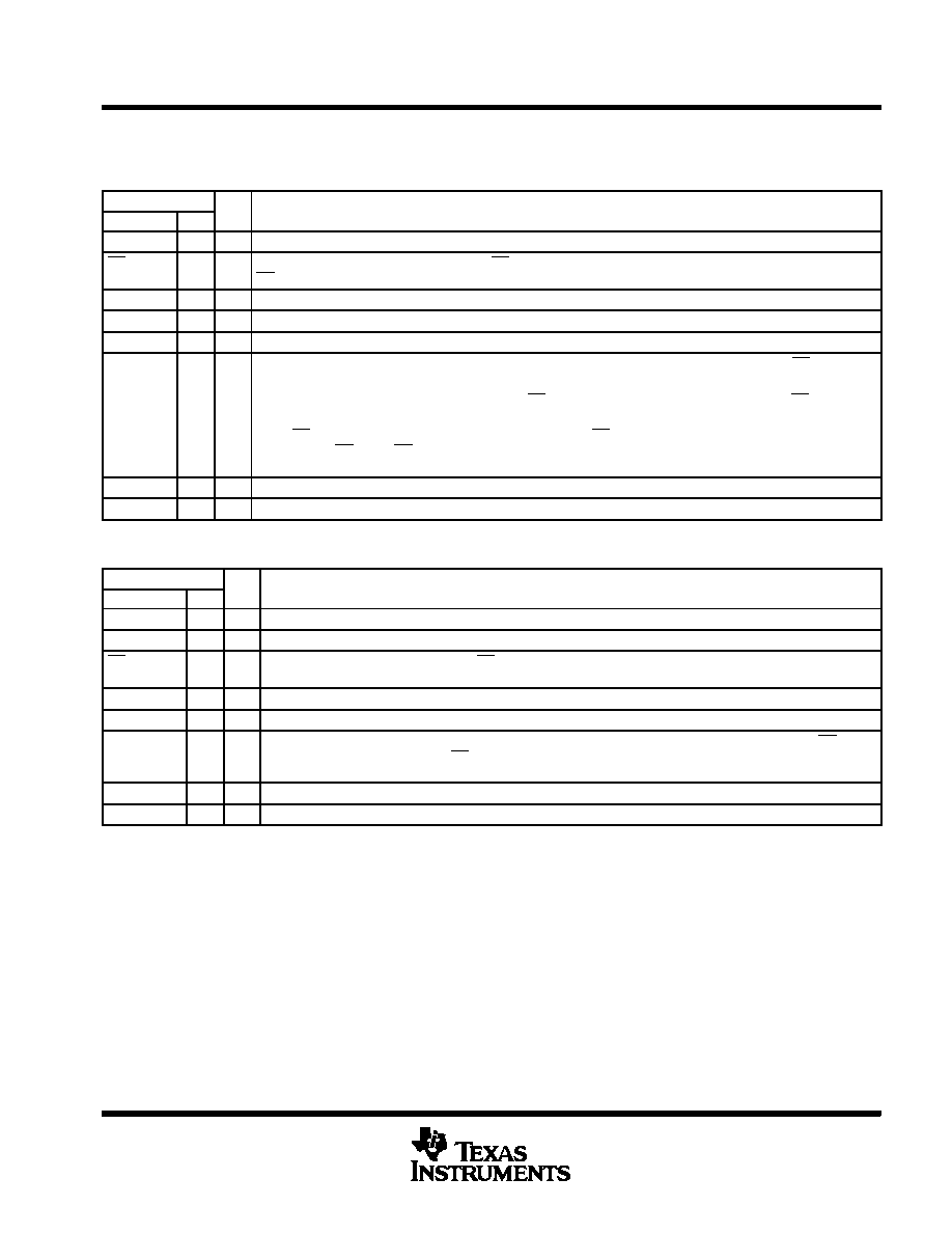
Terminal Functions
TLV2541
TERMINAL
I/O
DESCRIPTION
NAME
NO.
I/O
DESCRIPTION
AIN
4
I
Analog input channel
CS
1
I
Chip select. A high-to-low transition on the CS input removes SDO from 3-state within a maximum setup time.
CS can be used as the FS pin when a dedicated DSP serial port is used.
FS
7
I
DSP frame sync input. Indication of the start of a serial data frame. Tie this terminal to VDD if not used.
GND
3
I
Ground return for the internal circuitry. Unless otherwise noted, all voltage measurements are with respect to GND.
SCLK
5
I
Output serial clock. This terminal receives the serial SCLK from the host processor.
SDO
8
O
The 3-state serial output for the A/D conversion result. SDO is kept in the high-impedance state until CS falling edge
or FS rising edge, whichever occurs first. The output format is MSB first.
When FS is not used (FS = 1 at the falling edge of CS): The MSB is presented to the SDO pin after CS falling edge
and output data is valid on the first falling edge of SCLK.
When CS and FS are both used (FS = 0 at the falling edge of CS): The MSB is presented to the SDO pin after the
falling edge of CS. When CS is tied/held low, the MSB is presented on SDO after the rising FS. Output data is valid
on the first falling edge of SCLK. (This is typically used with an active FS from a DSP using a dedicated serial port.)
VDD
6
I
Positive supply voltage
VREF
2
I
External reference input
TLV2542/45
TERMINAL
I/O
DESCRIPTION
NAME
NO.
I/O
DESCRIPTION
AIN0 /AIN(+)
4
I
Analog input channel 0 for TLV2542—Positive input for TLV2545.
AIN1/AIN ()
5
I
Analog input channel 1 for TLV2542—Inverted input for TLV2545.
CS
1
I
Chip select. A high-to-low transition on CS removes SDO from 3-state within a maximum delay time. This pin can
be connected to the frame sync of a DSP using a dedicated serial port.
GND
3
I
Ground return for the internal circuitry. Unless otherwise noted, all voltage measurements are with respect to GND.
SCLK
7
I
Output serial clock. This terminal receives the serial SCLK from the host processor.
SDO
8
O
The 3-state serial output for the A/D conversion result. SDO is kept in the high-impedance state when CS is high
and presents output data after the CS falling edge until the LSB is presented. The output format is MSB first. SDO
returns to the Hi-Z state after the 16th SCLK. Output data is valid on the falling SCLK edge.
VDD
6
I
Positive supply voltage
VREF
2
I
External reference input
detailed description
The TLV2541, TLV2542, and TLV2545 are successive approximation (SAR) ADCs utilizing a charge
redistribution DAC. Figure 1 shows a simplified version of the ADC.
The sampling capacitor acquires the signal on AIN during the sampling period. When the conversion process
starts, the SAR control logic and charge redistribution DAC are used to add and subtract fixed amounts of charge
from the sampling capacitor to bring the comparator into a balanced condition. When the comparator is
balanced, the conversion is complete and the ADC output code is generated.
相關PDF資料 |
PDF描述 |
|---|---|
| TLV2542IDGK | 2-CH 12-BIT SUCCESSIVE APPROXIMATION ADC, SERIAL ACCESS, PDSO8 |
| TLV2542ID | 2-CH 12-BIT SUCCESSIVE APPROXIMATION ADC, SERIAL ACCESS, PDSO8 |
| TLV2542CDGKR | 2-CH 12-BIT SUCCESSIVE APPROXIMATION ADC, SERIAL ACCESS, PDSO8 |
| TLV2542IDGKR | 2-CH 12-BIT SUCCESSIVE APPROXIMATION ADC, SERIAL ACCESS, PDSO8 |
| TLV2542CDGKRG4 | 2-CH 12-BIT SUCCESSIVE APPROXIMATION ADC, SERIAL ACCESS, PDSO8 |
相關代理商/技術參數 |
參數描述 |
|---|---|
| TLV2542CDGKG4 | 功能描述:模數轉換器 - ADC 12-Bit 200 kSPS Serial Out RoHS:否 制造商:Texas Instruments 通道數量:2 結構:Sigma-Delta 轉換速率:125 SPs to 8 KSPs 分辨率:24 bit 輸入類型:Differential 信噪比:107 dB 接口類型:SPI 工作電源電壓:1.7 V to 3.6 V, 2.7 V to 5.25 V 最大工作溫度:+ 85 C 安裝風格:SMD/SMT 封裝 / 箱體:VQFN-32 |
| TLV2542CDGKR | 功能描述:模數轉換器 - ADC 12-Bit 200 kSPS Serial Out RoHS:否 制造商:Texas Instruments 通道數量:2 結構:Sigma-Delta 轉換速率:125 SPs to 8 KSPs 分辨率:24 bit 輸入類型:Differential 信噪比:107 dB 接口類型:SPI 工作電源電壓:1.7 V to 3.6 V, 2.7 V to 5.25 V 最大工作溫度:+ 85 C 安裝風格:SMD/SMT 封裝 / 箱體:VQFN-32 |
| TLV2542CDGKRG4 | 功能描述:模數轉換器 - ADC 12-Bit 200 kSPS Serial Out RoHS:否 制造商:Texas Instruments 通道數量:2 結構:Sigma-Delta 轉換速率:125 SPs to 8 KSPs 分辨率:24 bit 輸入類型:Differential 信噪比:107 dB 接口類型:SPI 工作電源電壓:1.7 V to 3.6 V, 2.7 V to 5.25 V 最大工作溫度:+ 85 C 安裝風格:SMD/SMT 封裝 / 箱體:VQFN-32 |
| TLV2542EVM | 功能描述:數據轉換 IC 開發工具 TLV2542 Eval Mod RoHS:否 制造商:Texas Instruments 產品:Demonstration Kits 類型:ADC 工具用于評估:ADS130E08 接口類型:SPI 工作電源電壓:- 6 V to + 6 V |
| TLV2542ID | 功能描述:模數轉換器 - ADC 12bit SAR ADC RoHS:否 制造商:Texas Instruments 通道數量:2 結構:Sigma-Delta 轉換速率:125 SPs to 8 KSPs 分辨率:24 bit 輸入類型:Differential 信噪比:107 dB 接口類型:SPI 工作電源電壓:1.7 V to 3.6 V, 2.7 V to 5.25 V 最大工作溫度:+ 85 C 安裝風格:SMD/SMT 封裝 / 箱體:VQFN-32 |
發布緊急采購,3分鐘左右您將得到回復。