- 您現在的位置:買賣IC網 > PDF目錄98251 > TLV2543IDBG4 (TEXAS INSTRUMENTS INC) 11-CH 12-BIT SUCCESSIVE APPROXIMATION ADC, SERIAL ACCESS, PDSO20 PDF資料下載
參數資料
| 型號: | TLV2543IDBG4 |
| 廠商: | TEXAS INSTRUMENTS INC |
| 元件分類: | ADC |
| 英文描述: | 11-CH 12-BIT SUCCESSIVE APPROXIMATION ADC, SERIAL ACCESS, PDSO20 |
| 封裝: | GREEN, PLASTIC, SSOP-20 |
| 文件頁數: | 22/28頁 |
| 文件大小: | 553K |
| 代理商: | TLV2543IDBG4 |
第1頁第2頁第3頁第4頁第5頁第6頁第7頁第8頁第9頁第10頁第11頁第12頁第13頁第14頁第15頁第16頁第17頁第18頁第19頁第20頁第21頁當前第22頁第23頁第24頁第25頁第26頁第27頁第28頁
TLV2543C, TLV2543I
12-BIT ANALOG-TO-DIGITAL CONVERTERS
WITH SERIAL CONTROL AND 11 ANALOG INPUTS
SLAS096C – MARCH 1995 – REVISED JUNE 2000
3
POST OFFICE BOX 655303
DALLAS, TEXAS 75265
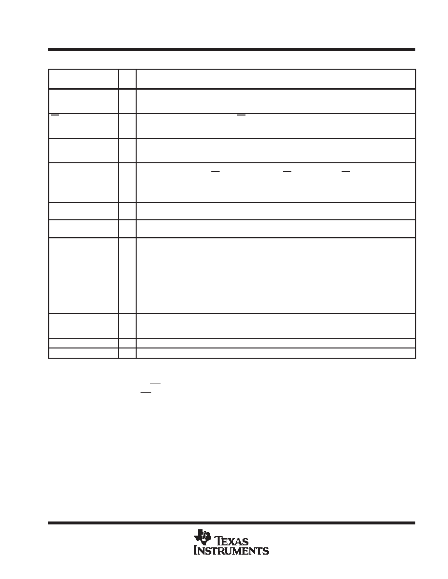
Terminal Functions
TERMINAL
I/O
DESCRIPTION
NAME
NO.
I/O
DESCRIPTION
AIN0 – AIN10
1–9,
11, 12
I
Analog input. These 11 analog-signal inputs are internally multiplexed. The driving source impedance should
be less than or equal to 50
for 4.1-MHz I/O CLOCK operation and capable of slewing the analog input
voltage into a capacitance of 60 pF.
CS
15
I
Chip select. A high-to-low transition on CS resets the internal counters and controls and enables DATA OUT,
DATA INPUT, and I/O CLOCK. A low-to-high transition disables DATA INPUT and I/O CLOCK within a setup
time.
DATA INPUT
17
I
Serial-data input. A 4-bit serial address selects the desired analog input or test voltage to be converted. The
serial data is presented with the MSB first and is shifted in on the first four rising edges of I/O CLOCK. After
the four address bits are read into the address register, I/O CLOCK clocks the remaining bits in order.
DATA OUT
16
O
Serial data output. This is the 3-state serial output for the A/D conversion result. DATA OUT is in the
high-impedance state when CS is high and active when CS is low. With a valid CS, DATA OUT is removed
from the high-impedance state and is driven to the logic level corresponding to the MSB/LSB value of the
previous conversion result. The next falling edge of I/O CLOCK drives DATA OUT to the logic level
corresponding to the next MSB / LSB, and the remaining bits are shifted out in order.
EOC
19
O
End of conversion. EOC goes from a high to a low logic level after the falling edge of the last I/O CLOCK and
remains low until the conversion is complete and data are ready for transfer.
GND
10
Ground. This is the ground return terminal for the internal circuitry. Unless otherwise noted, all voltage
measurements are with respect to GND.
I/O CLOCK
18
I
Input /output clock. I/O CLOCK receives the serial input and performs the following four functions:
1. It clocks the eight input data bits into the input data register on the first eight rising edges of I/O CLOCK
with the multiplexer address available after the fourth rising edge.
2. On the fourth falling edge of I/O CLOCK, the analog input voltage on the selected multiplexer input
begins charging the capacitor array and continues to do so until the last falling edge of I/O
CLOCK.
3. It shifts the 11 remaining bits of the previous conversion data out on DATA OUT. Data changes on
the falling edge of I/O CLOCK.
4. It transfers control of the conversion to the internal state controller on the falling edge of the last
I/O CLOCK.
REF +
14
I
Reference +. The upper reference voltage value (nominally VCC) is applied to REF+. The maximum input
voltage range is determined by the difference between the voltage applied to this terminal and the voltage
applied to the REF – terminal.
REF –
13
I
Reference –. The lower reference voltage value (nominally ground) is applied to REF –.
VCC
20
Positive supply voltage.
detailed description
Initially, with chip select (CS) high, I/O CLOCK and DATA INPUT are disabled and DATA OUT is in the
high-impedance state. CS, going low, begins the conversion sequence by enabling I/O CLOCK and DATA
INPUT and removes DATA OUT from the high-impedance state.
The input data is an 8-bit data stream consisting of a 4-bit analog channel address (D7 – D4), a 2-bit data length
select (D3 – D2), an output MSB or LSB first bit (D1), and a unipolar or bipolar output select bit (D0) that are
applied to DATA INPUT. The I/O CLOCK sequence applied to the I/O CLOCK terminal transfers this data to the
input data register.
During this transfer, the I/O CLOCK sequence also shifts the previous conversion result from the output data
register to DATA OUT. I/O CLOCK receives the input sequence of 8, 12, or 16 clocks long depending on the
data-length selection in the input data register. Sampling of the analog input begins on the fourth falling edge
of the input I/O CLOCK sequence and is held after the last falling edge of the I/O CLOCK sequence. The last
falling edge of the I/O CLOCK sequence also takes EOC low and begins the conversion.
相關PDF資料 |
PDF描述 |
|---|---|
| TLV2543CDWR | 11-CH 12-BIT SUCCESSIVE APPROXIMATION ADC, SERIAL ACCESS, PDSO20 |
| TLV2543IDWRG4 | 11-CH 12-BIT SUCCESSIVE APPROXIMATION ADC, SERIAL ACCESS, PDSO20 |
| TLV2543IN | 11-CH 12-BIT SUCCESSIVE APPROXIMATION ADC, SERIAL ACCESS, PDIP20 |
| TLV2543CDBG4 | 11-CH 12-BIT SUCCESSIVE APPROXIMATION ADC, SERIAL ACCESS, PDSO20 |
| TLV2543IDBR | 11-CH 12-BIT SUCCESSIVE APPROXIMATION ADC, SERIAL ACCESS, PDSO20 |
相關代理商/技術參數 |
參數描述 |
|---|---|
| TLV2543IDBR | 功能描述:模數轉換器 - ADC 12-Bit 66 kSPS Serial Out RoHS:否 制造商:Texas Instruments 通道數量:2 結構:Sigma-Delta 轉換速率:125 SPs to 8 KSPs 分辨率:24 bit 輸入類型:Differential 信噪比:107 dB 接口類型:SPI 工作電源電壓:1.7 V to 3.6 V, 2.7 V to 5.25 V 最大工作溫度:+ 85 C 安裝風格:SMD/SMT 封裝 / 箱體:VQFN-32 |
| TLV2543IDBRG4 | 功能描述:模數轉換器 - ADC 12-Bit 66 kSPS Serial Out RoHS:否 制造商:Texas Instruments 通道數量:2 結構:Sigma-Delta 轉換速率:125 SPs to 8 KSPs 分辨率:24 bit 輸入類型:Differential 信噪比:107 dB 接口類型:SPI 工作電源電壓:1.7 V to 3.6 V, 2.7 V to 5.25 V 最大工作溫度:+ 85 C 安裝風格:SMD/SMT 封裝 / 箱體:VQFN-32 |
| TLV2543IDW | 功能描述:模數轉換器 - ADC 12bit ADC w/11Chl RoHS:否 制造商:Texas Instruments 通道數量:2 結構:Sigma-Delta 轉換速率:125 SPs to 8 KSPs 分辨率:24 bit 輸入類型:Differential 信噪比:107 dB 接口類型:SPI 工作電源電壓:1.7 V to 3.6 V, 2.7 V to 5.25 V 最大工作溫度:+ 85 C 安裝風格:SMD/SMT 封裝 / 箱體:VQFN-32 |
| TLV2543IDWG4 | 功能描述:模數轉換器 - ADC 12bit ADC w/11Chl RoHS:否 制造商:Texas Instruments 通道數量:2 結構:Sigma-Delta 轉換速率:125 SPs to 8 KSPs 分辨率:24 bit 輸入類型:Differential 信噪比:107 dB 接口類型:SPI 工作電源電壓:1.7 V to 3.6 V, 2.7 V to 5.25 V 最大工作溫度:+ 85 C 安裝風格:SMD/SMT 封裝 / 箱體:VQFN-32 |
| TLV2543IDWR | 功能描述:模數轉換器 - ADC 12-Bit 66 kSPS Serial Out RoHS:否 制造商:Texas Instruments 通道數量:2 結構:Sigma-Delta 轉換速率:125 SPs to 8 KSPs 分辨率:24 bit 輸入類型:Differential 信噪比:107 dB 接口類型:SPI 工作電源電壓:1.7 V to 3.6 V, 2.7 V to 5.25 V 最大工作溫度:+ 85 C 安裝風格:SMD/SMT 封裝 / 箱體:VQFN-32 |
發布緊急采購,3分鐘左右您將得到回復。