- 您現(xiàn)在的位置:買賣IC網(wǎng) > PDF目錄98251 > TLV2548CPWR (TEXAS INSTRUMENTS INC) 8-CH 12-BIT SUCCESSIVE APPROXIMATION ADC, SERIAL ACCESS, PDSO20 PDF資料下載
參數(shù)資料
| 型號: | TLV2548CPWR |
| 廠商: | TEXAS INSTRUMENTS INC |
| 元件分類: | ADC |
| 英文描述: | 8-CH 12-BIT SUCCESSIVE APPROXIMATION ADC, SERIAL ACCESS, PDSO20 |
| 封裝: | GREEN, PLASTIC, TSSOP-20 |
| 文件頁數(shù): | 10/46頁 |
| 文件大小: | 1078K |
| 代理商: | TLV2548CPWR |
第1頁第2頁第3頁第4頁第5頁第6頁第7頁第8頁第9頁當(dāng)前第10頁第11頁第12頁第13頁第14頁第15頁第16頁第17頁第18頁第19頁第20頁第21頁第22頁第23頁第24頁第25頁第26頁第27頁第28頁第29頁第30頁第31頁第32頁第33頁第34頁第35頁第36頁第37頁第38頁第39頁第40頁第41頁第42頁第43頁第44頁第45頁第46頁
TLV2544, TLV2548
2.7V TO 5.5V, 12BIT, 200KSPS, 4/8CHANNEL, LOW POWER
SERIAL ANALOGTODIGITAL CONVERTERS WITH AUTOPOWERDOWN
SLAS198E FEBRUARY 1999 REVISED JUNE 2003
18
POST OFFICE BOX 655303
DALLAS, TEXAS 75265
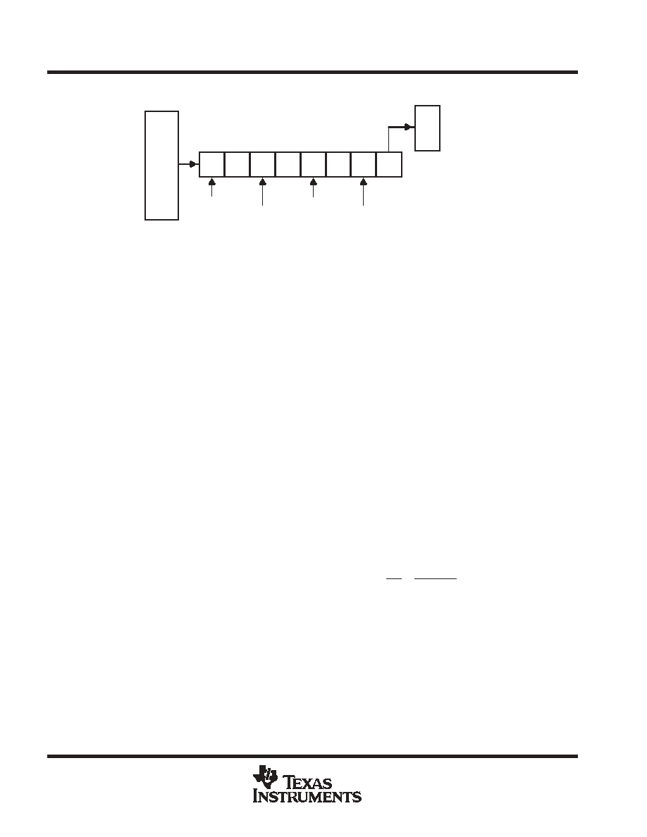
FIFO operation
76543210
ADC
12-BIT
×8
FIFO
SDO
Serial
FIFO Full
FIFO 3/4 Full
FIFO 1/2 Full
FIFO 1/4 Full
FIFO Threshold Pointer
Figure 15. TLV2544/TLV2548 FIFO
The device has an 8-layer FIFO that can be programmed for different thresholds. An interrupt is sent to the host
after the preprogrammed threshold is reached. The FIFO can be used to store data from either a fixed channel
or a series of channels based on a preprogrammed sweep sequence. For example, an application may require
eight measurements from channel 3. In this case, the FIFO is filled with eight data sequentially taken from
channel 3. Another application may require data from channel 0, channel 2, channel 4, and channel 6 in an
orderly manner. Therefore, the threshold is set for 1/2 and the sweep sequence 02460246 is chosen.
An interrupt is sent to the host as soon as all four data are in the FIFO.
In single shot mode, the FIFO automatically uses a 1/8 FIFO depth. Therefore the CFR bits (D1,0) controlling
FIFO depth are don’t care.
SCLK and conversion speed
There are two ways to adjust the conversion speed.
D The SCLK can be used as the source of the conversion clock to get the highest throughput of the device.
The minimum onboard OSC is 3.6 MHz and 14 conversion clocks are required to complete a conversion.
(Corresponding 3.86
s conversion time) The devices can operate with an SCLK up to 20 MHz for the
supply voltage range specified. When a more accurate conversion time is desired, the SCLK can be used as
the source of the conversion clock. The clock divider provides speed options appropriate for an application
where a high speed SCLK is used for faster I/O. The total conversion time is 14
× (DIV/fSCLK) where DIV is 1,
2, or 4. For example a 20 MHz SCLK with the divide by 4 option produces a {14
× (4/20 M)} = 2.8 s
conversion time. When an external serial clock (SCLK) is used as the source of the conversion clock, the
maximum equivalent conversion clock (fSCLK/DIV) should not exceed 6 MHz.
D Autopower down can be used to slow down the device at a reduced power consumption level. This mode
is always used by the converter. If the device is not accessed (by CS or CSTART), the converter is powered
down to save power. The built-in reference is left on in order to quickly resume operation within one half
SCLK period. This provides unlimited choices to trade speed with power savings.
reference voltage
The device has a built-in reference with a programmable level of 2 V or 4 V. If the internal reference is used,
REFP is set to 2 V or 4 V and REFM should be connected to the analog ground of the converter. An external
reference can also be used through two reference input pins, REFP and REFM, if the reference source is
programmed as external. The voltage levels applied to these pins establish the upper and lower limits of the
analog inputs to produce a full-scale and zero-scale reading respectively. The values of REFP, REFM, and the
analog input should not exceed the positive supply or be lower than GND consistent with the specified absolute
maximum ratings. The digital output is at full scale when the input signal is equal to or higher than REFP and
at zero when the input signal is equal to or lower than REFM.
相關(guān)PDF資料 |
PDF描述 |
|---|---|
| TLV2548CPWRG4 | 8-CH 12-BIT SUCCESSIVE APPROXIMATION ADC, SERIAL ACCESS, PDSO20 |
| TLV2548IDWG4 | 8-CH 12-BIT SUCCESSIVE APPROXIMATION ADC, SERIAL ACCESS, PDSO20 |
| TLV2548CDWG4 | 8-CH 12-BIT SUCCESSIVE APPROXIMATION ADC, SERIAL ACCESS, PDSO20 |
| TLV2548IDWRG4 | 8-CH 12-BIT SUCCESSIVE APPROXIMATION ADC, SERIAL ACCESS, PDSO20 |
| TLV2548IPWRG4 | 8-CH 12-BIT SUCCESSIVE APPROXIMATION ADC, SERIAL ACCESS, PDSO20 |
相關(guān)代理商/技術(shù)參數(shù) |
參數(shù)描述 |
|---|---|
| TLV2548CPWRG4 | 功能描述:模數(shù)轉(zhuǎn)換器 - ADC 12-Bit 200 kSPS Serial Out RoHS:否 制造商:Texas Instruments 通道數(shù)量:2 結(jié)構(gòu):Sigma-Delta 轉(zhuǎn)換速率:125 SPs to 8 KSPs 分辨率:24 bit 輸入類型:Differential 信噪比:107 dB 接口類型:SPI 工作電源電壓:1.7 V to 3.6 V, 2.7 V to 5.25 V 最大工作溫度:+ 85 C 安裝風(fēng)格:SMD/SMT 封裝 / 箱體:VQFN-32 |
| TLV2548EVM | 功能描述:EVALUATION MODULE FOR TLV2548 RoHS:是 類別:編程器,開發(fā)系統(tǒng) >> 評估板 - 模數(shù)轉(zhuǎn)換器 (ADC) 系列:- 產(chǎn)品培訓(xùn)模塊:Obsolescence Mitigation Program 標(biāo)準(zhǔn)包裝:1 系列:- ADC 的數(shù)量:1 位數(shù):12 采樣率(每秒):94.4k 數(shù)據(jù)接口:USB 輸入范圍:±VREF/2 在以下條件下的電源(標(biāo)準(zhǔn)):- 工作溫度:-40°C ~ 85°C 已用 IC / 零件:MAX11645 已供物品:板,軟件 |
| TLV2548IDW | 功能描述:模數(shù)轉(zhuǎn)換器 - ADC 12bit 200KSPS SAR RoHS:否 制造商:Texas Instruments 通道數(shù)量:2 結(jié)構(gòu):Sigma-Delta 轉(zhuǎn)換速率:125 SPs to 8 KSPs 分辨率:24 bit 輸入類型:Differential 信噪比:107 dB 接口類型:SPI 工作電源電壓:1.7 V to 3.6 V, 2.7 V to 5.25 V 最大工作溫度:+ 85 C 安裝風(fēng)格:SMD/SMT 封裝 / 箱體:VQFN-32 |
| TLV2548IDWG4 | 功能描述:模數(shù)轉(zhuǎn)換器 - ADC 12bit 200KSPS SAR RoHS:否 制造商:Texas Instruments 通道數(shù)量:2 結(jié)構(gòu):Sigma-Delta 轉(zhuǎn)換速率:125 SPs to 8 KSPs 分辨率:24 bit 輸入類型:Differential 信噪比:107 dB 接口類型:SPI 工作電源電壓:1.7 V to 3.6 V, 2.7 V to 5.25 V 最大工作溫度:+ 85 C 安裝風(fēng)格:SMD/SMT 封裝 / 箱體:VQFN-32 |
| TLV2548IDWR | 功能描述:模數(shù)轉(zhuǎn)換器 - ADC 12-Bit 200 kSPS Serial Out RoHS:否 制造商:Texas Instruments 通道數(shù)量:2 結(jié)構(gòu):Sigma-Delta 轉(zhuǎn)換速率:125 SPs to 8 KSPs 分辨率:24 bit 輸入類型:Differential 信噪比:107 dB 接口類型:SPI 工作電源電壓:1.7 V to 3.6 V, 2.7 V to 5.25 V 最大工作溫度:+ 85 C 安裝風(fēng)格:SMD/SMT 封裝 / 箱體:VQFN-32 |
發(fā)布緊急采購,3分鐘左右您將得到回復(fù)。