- 您現在的位置:買賣IC網 > PDF目錄98255 > TLV5535IPWG4 (TEXAS INSTRUMENTS INC) 1-CH 8-BIT PROPRIETARY METHOD ADC, PARALLEL ACCESS, PDSO28 PDF資料下載
參數資料
| 型號: | TLV5535IPWG4 |
| 廠商: | TEXAS INSTRUMENTS INC |
| 元件分類: | ADC |
| 英文描述: | 1-CH 8-BIT PROPRIETARY METHOD ADC, PARALLEL ACCESS, PDSO28 |
| 封裝: | GREEN, PLASTIC, TSSOP-28 |
| 文件頁數: | 23/35頁 |
| 文件大小: | 723K |
| 代理商: | TLV5535IPWG4 |
第1頁第2頁第3頁第4頁第5頁第6頁第7頁第8頁第9頁第10頁第11頁第12頁第13頁第14頁第15頁第16頁第17頁第18頁第19頁第20頁第21頁第22頁當前第23頁第24頁第25頁第26頁第27頁第28頁第29頁第30頁第31頁第32頁第33頁第34頁第35頁
TLV5535
8-BIT, 35 MSPS, LOW-POWER ANALOG-TO-DIGITAL CONVERTER
SLAS221 – JUNE 1999
3
POST OFFICE BOX 655303
DALLAS, TEXAS 75265
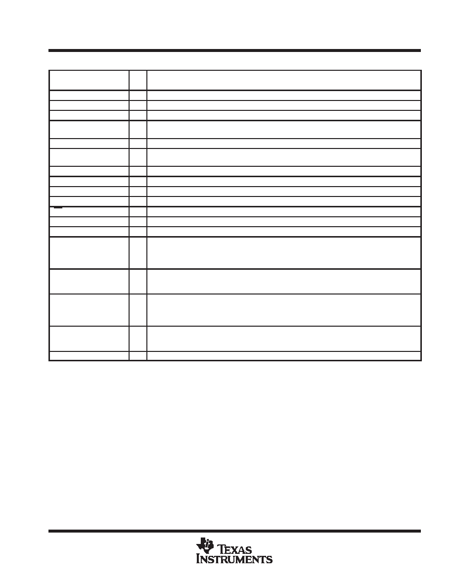
Terminal Functions
TERMINAL
I/O
DESCRIPTION
NAME
NO.
I/O
DESCRIPTION
AIN
26
I
Analog input
AVDD
16, 27
I
Analog supply voltage
AVSS
18, 23, 28
I
Analog ground
BG
17
O
Band gap reference voltage. A 1-
F capacitor (with an optional 0.1-F capacitor in parallel) should be
connected between this terminal and AVSS for external filtering.
CLK
12
I
Clock input. The input is sampled on each rising edge of CLK.
CML
25
O
Common mode level. This voltage is equal to (AVDD – AVSS) ÷ 2. An external 0.1-F capacitor should be
connected between this terminal and AVSS.
D0 – D7
2 – 9
O
Data outputs. D7 is the MSB.
DRVDD
1
I
Supply voltage for digital output drivers
DRVSS
10
I
Ground for digital output drivers
DVDD
14
I
Digital supply voltage
OE
13
I
Output enable. When high, the D0 – D7 outputs go in high-impedance mode.
DVSS
11
I
Digital ground
PWDN_REF
24
I
Power down for internal reference voltages. A high on this terminal disables the internal reference circuit.
REFBI
21
I
Reference voltage bottom input. The voltage at this terminal defines the bottom reference voltage for the
ADC. It can be connected to REFBO or to an externally generated reference level. Sufficient filtering
should be applied to this input. The use of a 0.1-
F capacitor connected between REFBI and AVSS is
recommended. Additionaly, a 0.1-
F capacitor can be connected between REFTI and REFBI.
REFBO
22
O
Reference voltage bottom output. An internally generated reference is available at this terminal. It can be
connected to REFBI or left unconnected. A 1-
F capacitor between REFBO and AVSS provides sufficient
decoupling required for this output.
REFTI
20
I
Reference voltage top input. The voltage at this terminal defines the top reference voltage for the ADC.
It can be connected to REFTO or to an externally generated reference level. Sufficient filtering should be
applied to this input. The use of a 0.1-
F capacitor between REFTI and AVSS is recommended.
Additionaly, a 0.1-
F capacitor can be connected between REFTI and REFBI.
REFTO
19
O
Reference voltage top output. An internally generated reference is available at this terminal. It can be
connected to REFTI or left unconnected. A 1-
F capacitor between REFTO and AVSS provides sufficient
decoupling required for this output.
STBY
15
I
Standby input. A high level on this input enables power-down mode.
absolute maximum ratings over operating free-air temperature (unless otherwise noted)
Supply voltage range: AVDD to AVSS, DVDD to DVSS
– 0.5 V to 4.5 V
. . . . . . . . . . . . . . . . . . . . . . . . . . . . . . . . . .
AVDD to DVDD, AVSS to DVSS
– 0.5 V to 0.5 V
. . . . . . . . . . . . . . . . . . . . . . . . . . . . . . . . . .
Digital input voltage range to DVSS
– 0.5 V to DVDD + 0.5 V
. . . . . . . . . . . . . . . . . . . . . . . . . . . . . . . . . . . . . . . . . .
Analog input voltage range to AVSS
– 0.5 V to AVDD + 0.5 V
. . . . . . . . . . . . . . . . . . . . . . . . . . . . . . . . . . . . . . . . .
Digital output voltage range applied from external source to DGND
– 0.5 V to DVDD + 0.5 V
. . . . . . . . . . . . . .
Reference voltage input range to AGND: V(REFTI), V(REFTO), V(REFBI), V(REFBO) –0.5 V to AVDD + 0.5 V
Operating free-air temperature range, TA: TLV5535I
–40
°C to 85°C
. . . . . . . . . . . . . . . . . . . . . . . . . . . . . . . . . .
Storage temperature range, Tstg
–55
°C to 150°C
. . . . . . . . . . . . . . . . . . . . . . . . . . . . . . . . . . . . . . . . . . . . . . . . . . .
Stresses beyond those listed under “absolute maximum ratings” may cause permanent damage to the device. These are stress ratings only, and
functional operation of the device at these or any other conditions beyond those indicated under “recommended operating conditions” is not
implied. Exposure to absolute-maximum-rated conditions for extended periods may affect device reliability.
相關PDF資料 |
PDF描述 |
|---|---|
| TLV5535IPW | 1-CH 8-BIT PROPRIETARY METHOD ADC, PARALLEL ACCESS, PDSO28 |
| TLV5540CPW | 1-CH 8-BIT FLASH METHOD ADC, PARALLEL ACCESS, PDSO24 |
| TLV5540INSLE | 1-CH 8-BIT FLASH METHOD ADC, PARALLEL ACCESS, PDSO24 |
| TLV5540IPW | 1-CH 8-BIT FLASH METHOD ADC, PARALLEL ACCESS, PDSO24 |
| TLV5540CNSLE | 1-CH 8-BIT FLASH METHOD ADC, PARALLEL ACCESS, PDSO24 |
相關代理商/技術參數 |
參數描述 |
|---|---|
| TLV5535IPWR | 功能描述:模數轉換器 - ADC 8 Bit 35 MSPS Single Ch. Low Pwr RoHS:否 制造商:Texas Instruments 通道數量:2 結構:Sigma-Delta 轉換速率:125 SPs to 8 KSPs 分辨率:24 bit 輸入類型:Differential 信噪比:107 dB 接口類型:SPI 工作電源電壓:1.7 V to 3.6 V, 2.7 V to 5.25 V 最大工作溫度:+ 85 C 安裝風格:SMD/SMT 封裝 / 箱體:VQFN-32 |
| TLV5535IPWRG4 | 功能描述:模數轉換器 - ADC 8 Bit 35 MSPS Single Ch. Low Pwr RoHS:否 制造商:Texas Instruments 通道數量:2 結構:Sigma-Delta 轉換速率:125 SPs to 8 KSPs 分辨率:24 bit 輸入類型:Differential 信噪比:107 dB 接口類型:SPI 工作電源電壓:1.7 V to 3.6 V, 2.7 V to 5.25 V 最大工作溫度:+ 85 C 安裝風格:SMD/SMT 封裝 / 箱體:VQFN-32 |
| TLV5535IPWRG4Q1 | 功能描述:模數轉換器 - ADC 8 Bit 35MSPS ADC Sgl Ch Low Pwr RoHS:否 制造商:Texas Instruments 通道數量:2 結構:Sigma-Delta 轉換速率:125 SPs to 8 KSPs 分辨率:24 bit 輸入類型:Differential 信噪比:107 dB 接口類型:SPI 工作電源電壓:1.7 V to 3.6 V, 2.7 V to 5.25 V 最大工作溫度:+ 85 C 安裝風格:SMD/SMT 封裝 / 箱體:VQFN-32 |
| TLV5535IPWRQ1 | 功能描述:模數轉換器 - ADC Auto Cat 8B 35MSPS ADC Sgl Ch. Lo Pwr RoHS:否 制造商:Texas Instruments 通道數量:2 結構:Sigma-Delta 轉換速率:125 SPs to 8 KSPs 分辨率:24 bit 輸入類型:Differential 信噪比:107 dB 接口類型:SPI 工作電源電壓:1.7 V to 3.6 V, 2.7 V to 5.25 V 最大工作溫度:+ 85 C 安裝風格:SMD/SMT 封裝 / 箱體:VQFN-32 |
| TLV5535PW | 制造商:TI 制造商全稱:Texas Instruments 功能描述:8-BIT, 35 MSPS, LOW-POWER ANALOG-TO-DIGITAL CONVERTER |
發布緊急采購,3分鐘左右您將得到回復。