- 您現在的位置:買賣IC網 > PDF目錄98257 > TLV5613IDWG4 (TEXAS INSTRUMENTS INC) PARALLEL, WORD INPUT LOADING, 1 us SETTLING TIME, 12-BIT DAC, PDSO20 PDF資料下載
參數資料
| 型號: | TLV5613IDWG4 |
| 廠商: | TEXAS INSTRUMENTS INC |
| 元件分類: | DAC |
| 英文描述: | PARALLEL, WORD INPUT LOADING, 1 us SETTLING TIME, 12-BIT DAC, PDSO20 |
| 封裝: | PLASTIC, SO-20 |
| 文件頁數: | 5/23頁 |
| 文件大小: | 447K |
| 代理商: | TLV5613IDWG4 |
TLV5613
2.7 V TO 5.5 V 12-BIT PARALLEL DIGITAL-TO-ANALOG CONVERTER
WITH POWER DOWN
SLAS174B – DECEMBER 1997 – REVISED NOVEMBER 2000
13
POST OFFICE BOX 655303
DALLAS, TEXAS 75265
APPLICATION INFORMATION
layout considerations
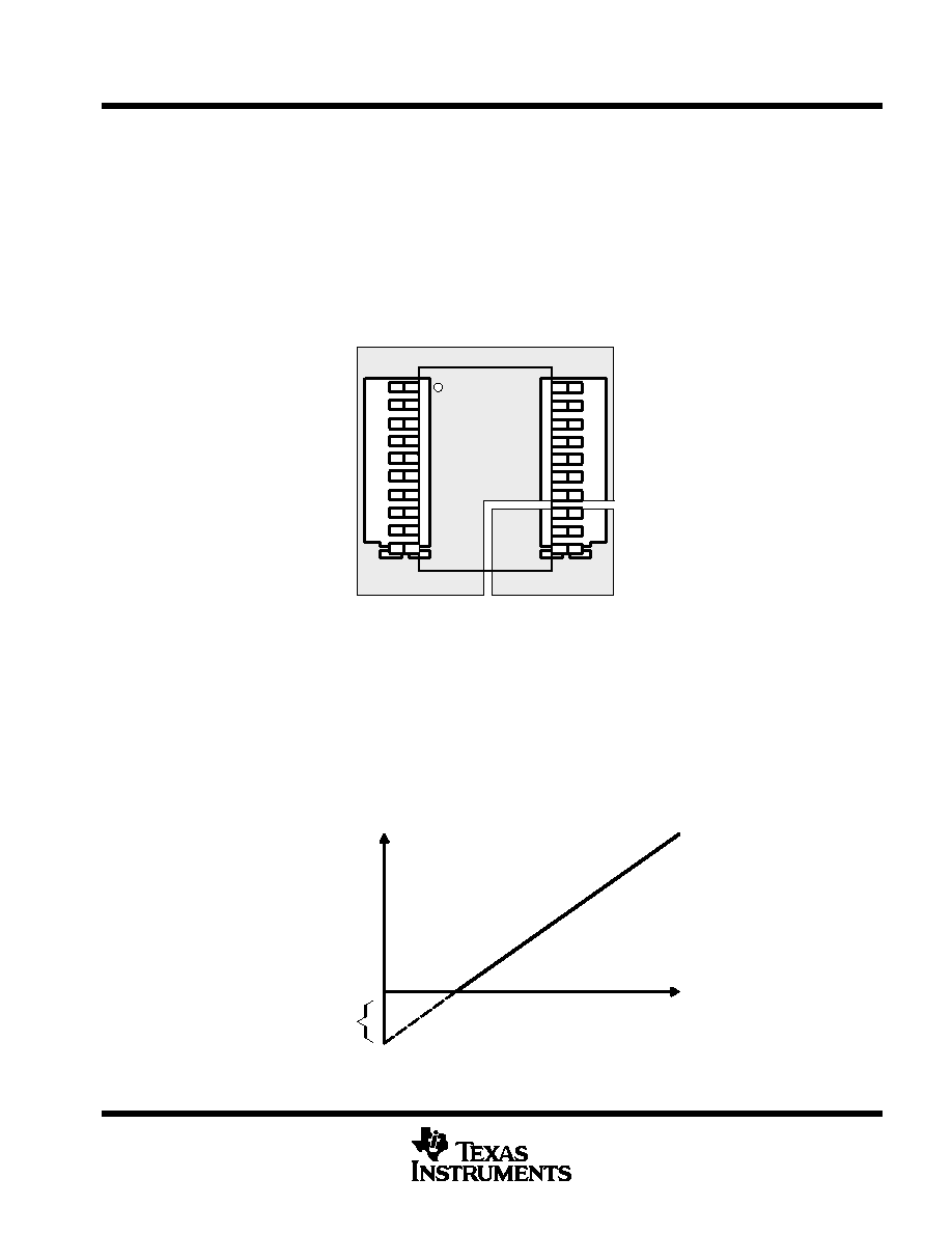
To achieve the best performance, it is recommended to have separate power planes for GND, AVDD, and DVDD.
Figure 15 shows how to lay out the power planes for the TLV5613. As a general rule, digital and analog signals
should be separated as wide as possible. To avoid crosstalk, analog and digital traces must not be routed in
parallel. The two positive power planes ( AVDD and DVDD) should be connected together at one point with a
ferrite bead.
A 100-nF ceramic low series inductance capacitor between DVDD and GND and a 1-F tantalum capacitor
between AVDD and GND as close as possible to the supply pins are recommended for optimal performance.
DVDD
AVDD
Figure 15. TLV5613 Board Layout
linearity, offset, and gain error using single end supplies
When an amplifier is operated from a single supply, the voltage offset can still be either positive or negative. With
a positive offset, the output voltage changes on the first code change. With a negative offset the output voltage
may not change with the first code depending on the magnitude of the offset voltage.
The output amplifier attempts to drive the output to a negative voltage. However, because the most negative
supply rail is ground, the output cannot drive below ground and clamps the output at 0 V.
The output voltage remains at zero until the input code value produces a sufficient positive output voltage to
overcome the negative offset voltage, resulting in the transfer function shown in Figure 16.
DAC Code
Output
Voltage
0 V
Negative
Offset
Figure 16. Effect of Negative Offset (Single Supply)
相關PDF資料 |
PDF描述 |
|---|---|
| TLV5613CPWRG4 | PARALLEL, WORD INPUT LOADING, 1 us SETTLING TIME, 12-BIT DAC, PDSO20 |
| TLV5614CDRG4 | SERIAL INPUT LOADING, 9 us SETTLING TIME, 12-BIT DAC, PDSO16 |
| TLV5614IDR | SERIAL INPUT LOADING, 9 us SETTLING TIME, 12-BIT DAC, PDSO16 |
| TLV5614CPW | SERIAL INPUT LOADING, 9 us SETTLING TIME, 12-BIT DAC, PDSO16 |
| TLV5614IPW | SERIAL INPUT LOADING, 9 us SETTLING TIME, 12-BIT DAC, PDSO16 |
相關代理商/技術參數 |
參數描述 |
|---|---|
| TLV5613IDWR | 功能描述:數模轉換器- DAC 12-Bit DAC Parallel Voltage Out RoHS:否 制造商:Texas Instruments 轉換器數量:1 DAC 輸出端數量:1 轉換速率:2 MSPs 分辨率:16 bit 接口類型:QSPI, SPI, Serial (3-Wire, Microwire) 穩定時間:1 us 最大工作溫度:+ 85 C 安裝風格:SMD/SMT 封裝 / 箱體:SOIC-14 封裝:Tube |
| TLV5613IDWRG4 | 功能描述:數模轉換器- DAC 12-Bit DAC Parallel Voltage Out RoHS:否 制造商:Texas Instruments 轉換器數量:1 DAC 輸出端數量:1 轉換速率:2 MSPs 分辨率:16 bit 接口類型:QSPI, SPI, Serial (3-Wire, Microwire) 穩定時間:1 us 最大工作溫度:+ 85 C 安裝風格:SMD/SMT 封裝 / 箱體:SOIC-14 封裝:Tube |
| TLV5613IPW | 功能描述:數模轉換器- DAC 12bit CMOS DAC RoHS:否 制造商:Texas Instruments 轉換器數量:1 DAC 輸出端數量:1 轉換速率:2 MSPs 分辨率:16 bit 接口類型:QSPI, SPI, Serial (3-Wire, Microwire) 穩定時間:1 us 最大工作溫度:+ 85 C 安裝風格:SMD/SMT 封裝 / 箱體:SOIC-14 封裝:Tube |
| TLV5613IPWG4 | 功能描述:數模轉換器- DAC 12-Bit DAC Parallel Voltage Out RoHS:否 制造商:Texas Instruments 轉換器數量:1 DAC 輸出端數量:1 轉換速率:2 MSPs 分辨率:16 bit 接口類型:QSPI, SPI, Serial (3-Wire, Microwire) 穩定時間:1 us 最大工作溫度:+ 85 C 安裝風格:SMD/SMT 封裝 / 箱體:SOIC-14 封裝:Tube |
| TLV5613IPWR | 功能描述:數模轉換器- DAC 12-Bit DAC Parallel Voltage Out RoHS:否 制造商:Texas Instruments 轉換器數量:1 DAC 輸出端數量:1 轉換速率:2 MSPs 分辨率:16 bit 接口類型:QSPI, SPI, Serial (3-Wire, Microwire) 穩定時間:1 us 最大工作溫度:+ 85 C 安裝風格:SMD/SMT 封裝 / 箱體:SOIC-14 封裝:Tube |
發布緊急采購,3分鐘左右您將得到回復。