- 您現在的位置:買賣IC網 > PDF目錄382648 > TMX320F2810GHHA (Texas Instruments, Inc.) DIGITAL SIGNAL PROCESSORS PDF資料下載
參數資料
| 型號: | TMX320F2810GHHA |
| 廠商: | Texas Instruments, Inc. |
| 元件分類: | 數字信號處理 |
| 英文描述: | DIGITAL SIGNAL PROCESSORS |
| 中文描述: | 數字信號處理器 |
| 文件頁數: | 39/103頁 |
| 文件大小: | 1341K |
| 代理商: | TMX320F2810GHHA |
第1頁第2頁第3頁第4頁第5頁第6頁第7頁第8頁第9頁第10頁第11頁第12頁第13頁第14頁第15頁第16頁第17頁第18頁第19頁第20頁第21頁第22頁第23頁第24頁第25頁第26頁第27頁第28頁第29頁第30頁第31頁第32頁第33頁第34頁第35頁第36頁第37頁第38頁當前第39頁第40頁第41頁第42頁第43頁第44頁第45頁第46頁第47頁第48頁第49頁第50頁第51頁第52頁第53頁第54頁第55頁第56頁第57頁第58頁第59頁第60頁第61頁第62頁第63頁第64頁第65頁第66頁第67頁第68頁第69頁第70頁第71頁第72頁第73頁第74頁第75頁第76頁第77頁第78頁第79頁第80頁第81頁第82頁第83頁第84頁第85頁第86頁第87頁第88頁第89頁第90頁第91頁第92頁第93頁第94頁第95頁第96頁第97頁第98頁第99頁第100頁第101頁第102頁第103頁
TMS320F2810, TMS320F2812
DIGITAL SIGNAL PROCESSORS
SPRS174B
–
APRIL 2001
–
REVISED SEPTEMBER 2001
39
POST OFFICE BOX 1443
HOUSTON, TEXAS 77251
–
1443
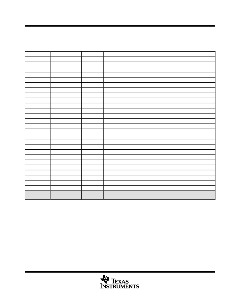
PIE registers
The registers controlling the functionality of the PIE block are listed in Table 22.
Table 22. PIE Configurations and Control Register Mappings
NAME
ADDRESS
SIZE (x16)
DESCRIPTION
PIECTRL
0x0000
–
0CE0
1
PIE, Control Register
PIEACK
0x0000
–
0CE1
1
PIE, Acknowledge Register
PIEIER1
0x0000
–
0CE2
1
PIE, INT1 Group Enable Register
PIEIFR1
0x0000
–
0CE3
1
PIE, INT1 Group Flag Register
PIEIER2
0x0000
–
0CE4
1
PIE, INT2 Group Enable Register
PIEIFR2
0x0000
–
0CE5
1
PIE, INT2 Group Flag Register
PIEIER3
0x0000
–
0CE6
1
PIE, INT3 Group Enable Register
PIEIFR3
0x0000
–
0CE7
1
PIE, INT3 Group Flag Register
PIEIER4
0x0000
–
0CE8
1
PIE, INT4 Group Enable Register
PIEIFR4
0x0000
–
0CE9
1
PIE, INT4 Group Flag Register
PIEIER5
0x0000
–
0CEA
1
PIE, INT5 Group Enable Register
PIEIFR5
0x0000
–
0CEB
1
PIE, INT5 Group Flag Register
PIEIER6
0x0000
–
0CEC
1
PIE, INT6 Group Enable Register
PIEIFR6
0x0000
–
0CED
1
PIE, INT6 Group Flag Register
PIEIER7
0x0000
–
0CEE
1
PIE, INT7 Group Enable Register
PIEIFR7
0x0000
–
0CEF
1
PIE, INT7 Group Flag Register
PIEIER8
0x0000
–
0CF0
1
PIE, INT8 Group Enable Register
PIEIFR8
0x0000
–
0CF1
1
PIE, INT8 Group Flag Register
PIEIER9
0x0000
–
0CF2
1
PIE, INT9 Group Enable Register
PIEIFR9
0x0000
–
0CF3
1
PIE, INT9 Group Flag Register
PIEIER10
0x0000
–
0CF4
1
PIE, INT10 Group Enable Register
PIEIFR10
0x0000
–
0CF5
1
PIE, INT10 Group Flag Register
PIEIER11
0x0000
–
0CF6
1
PIE, INT11 Group Enable Register
PIEIFR11
0x0000
–
0CF7
1
PIE, INT11 Group Flag Register
PIEIER12
0x0000
–
0CF8
1
PIE, INT12 Group Enable Register
PIEIFR12
0x0000
–
0CF9
1
PIE, INT12 Group Flag Register
reserved
0x0000
–
0CFA
0x0000
–
0CFF
6
reserved
The PIE configuration and control registers are not protected by EALLOW mode. The PIE vector table is protected.
P
相關PDF資料 |
PDF描述 |
|---|---|
| TMX320F2810PBKA | DIGITAL SIGNAL PROCESSORS |
| TMP320F2810PBKA | DIGITAL SIGNAL PROCESSORS |
| TMX320F2810PBKAEP | Digital Signal Processors |
| TMP320F2810PBKAEP | Digital Signal Processors |
| TMX320F2810PBKS | DIGITAL SIGNAL PROCESSORS |
相關代理商/技術參數 |
參數描述 |
|---|---|
| TMX320F2810GHHMEP | 制造商:TI 制造商全稱:Texas Instruments 功能描述:Digital Signal Processors |
| TMX320F2810GHHS | 制造商:TI 制造商全稱:Texas Instruments 功能描述:DIGITAL SIGNAL PROCESSORS |
| TMX320F2810PBKA | 制造商:TI 制造商全稱:Texas Instruments 功能描述:DIGITAL SIGNAL PROCESSORS |
| TMX320F2810PBKAEP | 制造商:TI 制造商全稱:Texas Instruments 功能描述:Digital Signal Processors |
| TMX320F2810PBKS | 制造商:TI 制造商全稱:Texas Instruments 功能描述:DIGITAL SIGNAL PROCESSORS |
發布緊急采購,3分鐘左右您將得到回復。