- 您現在的位置:買賣IC網 > PDF目錄382662 > TOP245R-TL SMPS Controller PDF資料下載
參數資料
| 型號: | TOP245R-TL |
| 英文描述: | SMPS Controller |
| 中文描述: | 開關電源控制器 |
| 文件頁數: | 8/52頁 |
| 文件大小: | 457K |
| 代理商: | TOP245R-TL |
第1頁第2頁第3頁第4頁第5頁第6頁第7頁當前第8頁第9頁第10頁第11頁第12頁第13頁第14頁第15頁第16頁第17頁第18頁第19頁第20頁第21頁第22頁第23頁第24頁第25頁第26頁第27頁第28頁第29頁第30頁第31頁第32頁第33頁第34頁第35頁第36頁第37頁第38頁第39頁第40頁第41頁第42頁第43頁第44頁第45頁第46頁第47頁第48頁第49頁第50頁第51頁第52頁
TOP242-250
8
H
9/02
General Information & Table of Contents
voltage rating of the MOSFET (700 V), due to the absence of
the reflected voltage and leakage spikes on the drain. A small
amount of hysteresis is provided on the OV threshold to
prevent noise triggering. The OV feature can be disabled
independent of the UV feature as shown in Figures 18 and 32.
Data Sheets 2
reduces power supply output sensitivity to line transients. This
feed forward operation is illustrated in Figure 7 by the
different values of I
(Y, R or F package) or I
(P or G Pack-
age). Note that for the same CONTROL pin current, higher
line voltage results in smaller operating duty cycle. As an added
feature, the maximum duty cycle DC
is also reduced from
78% (typical) at a voltage slightly higher than the UV thresh-
old to 30% (typical) at the OV threshold (see Figures 7 and
11). Limiting DC
MAX
at higher line voltages helps
Package Information 7
DPA-SwitchDC-DC Seminar 8
LinkSwitch & TinySwitch-IIAC-DC Seminar 9
TOPSwitch-GXAC-DC Seminar 10
Sales Representatives and Distributors 11
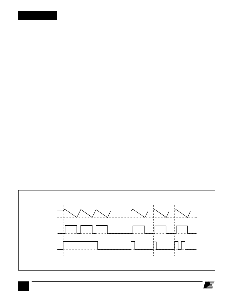
Figure 10. Synchronization Timing Diagram.
PI-2637-060600
Oscillator
(SAW)
DMAX
Enable from
X, L or M Pin (STOP)
Time
CURRENT LIMIT (X) pin (Y, R or F package) or MULTI-
FUNCTION (M) pin (P or G package) and the rectified DC
high voltage bus, the current limit is reduced with increasing
line voltage, allowing a true power limiting operation against
line variation to be implemented. When using an RCD clamp,
this power limiting technique reduces maximum clamp
voltage at high line. This allows for higher reflected voltage
designs as well as reducing clamp dissipation.
The leading edge blanking circuit inhibits the current limit
comparator for a short time after the output MOSFET is turned
on. The leading edge blanking time has been set so that, if a
power supply is designed properly, current spikes caused by
primary-side capacitances and secondary-side rectifier reverse
recovery time should not cause premature termination of the
switching pulse.
The current limit is lower for a short period after the leading
edge blanking time as shown in Figure 52. This is due to
dynamic characteristics of the MOSFET. To avoid triggering
the current limit in normal operation, the drain current wave-
form should stay within the envelope shown.
Line Under-Voltage Detection (UV)
At power up, UV keeps
TOPSwitch-GX
off until the input line
voltage reaches the under voltage threshold. At power down,
UV prevents auto-restart attempts after the output goes out of
regulation. This eliminates power down glitches caused by
the slow discharge of large input storage capacitor present in
applications such as standby supplies. A single resistor
connected from the LINE-SENSE pin (Y, R or F package) or
MULTI-FUNCTION pin (P or G package) to the rectified DC
high voltage bus sets UV threshold during power up. Once the
power supply is successfully turned on, the UV threshold is
lowered to 40% of the initial UV threshold to allow extended
input voltage operating range (UV low threshold). If the UV
low threshold is reached during operation without the power
supply losing regulation the device will turn off and stay off
until UV (high threshold) has been reached again. If the power
supply loses regulation before reaching the UV low threshold,
the device will enter auto-restart. At the end of each auto-
restart cycle (S7), the UV comparator is enabled. If the UV high
threshold is not exceeded the MOSFET will be disabled during
the next cycle (see Figure 8). The UV feature can be disabled
independent of OV feature as shown in Figures 19 and 23.
Line Overvoltage Shutdown (OV)
The same resistor used for UV also sets an overvoltage thresh-
old which, once exceeded, will force
TOPSwitch-GX
output
into off-state. The ratio of OV and UV thresholds is preset at
4.5 as can be seen in Figure 11. When the MOSFET is off, the
rectified DC high voltage surge capability is increased to the
Line Feed Forward with DC
Reduction
The same resistor used for UV and OV also
implements line
voltage feed forward which minimizes output line ripple and
相關PDF資料 |
PDF描述 |
|---|---|
| TOP250R | Up to 290 W Extended power. design flexible. |
| TOP245P | Up to 290 W Extended power. design flexible. |
| TOPD345-RX5 | Optoelectronic |
| TOPD346-RXMS | Optoelectronic |
| TOPD347-RXB | Telecommunication IC |
相關代理商/技術參數 |
參數描述 |
|---|---|
| TOP245Y | 功能描述:IC OFFLINE SWIT UVLO HV TO220 RoHS:否 類別:集成電路 (IC) >> PMIC - AC-DC 轉換器,離線開關 系列:TOPSwitch®-GX 標準包裝:1 系列:FPS™ 輸出隔離:隔離 頻率范圍:61kHz ~ 73kHz 輸入電壓:8 V ~ 26 V 輸出電壓:650V 功率(瓦特):12W 工作溫度:-40°C ~ 115°C 封裝/外殼:8-DIP(0.300",7.62mm) 供應商設備封裝:8-MDIP 包裝:Digi-Reel® 其它名稱:FSL206MRBNFSDKR |
| TOP245Y- | 制造商:POWERINT 制造商全稱:Power Integrations, Inc. 功能描述:TOPSwitch-GX Family Extended Power, Design Flexible, EcoSmart, Integrated Off-line Switcher |
| TOP245Y/F | 制造商:未知廠家 制造商全稱:未知廠家 功能描述:Up to 290 W Extended power. design flexible. |
| TOP245YN | 功能描述:交流/直流開關轉換器 60W 85-265 VAC 85 W 230 VAC RoHS:否 制造商:STMicroelectronics 輸出電壓:800 V 輸入/電源電壓(最大值):23.5 V 輸入/電源電壓(最小值):11.5 V 開關頻率:115 kHz 電源電流:1.6 mA 工作溫度范圍:- 40 C to + 150 C 安裝風格:SMD/SMT 封裝 / 箱體:SSO-10 封裝:Reel |
| TOP245YN- | 制造商:POWERINT 制造商全稱:Power Integrations, Inc. 功能描述:TOPSwitch-GX Family Extended Power, Design Flexible, EcoSmart, Integrated Off-line Switcher |
發布緊急采購,3分鐘左右您將得到回復。