- 您現在的位置:買賣IC網 > PDF目錄98271 > TPA2037D1YFFT (TEXAS INSTRUMENTS INC) 3.24 W, 1 CHANNEL, AUDIO AMPLIFIER, BGA9 PDF資料下載
參數資料
| 型號: | TPA2037D1YFFT |
| 廠商: | TEXAS INSTRUMENTS INC |
| 元件分類: | 音頻/視頻放大 |
| 英文描述: | 3.24 W, 1 CHANNEL, AUDIO AMPLIFIER, BGA9 |
| 封裝: | 1.21 X 1.16 MM, 0.40 MM PITCH, LEAD FREE, WCSP-9 |
| 文件頁數: | 6/20頁 |
| 文件大小: | 597K |
| 代理商: | TPA2037D1YFFT |
SLOS648B – OCTOBER 2009 – REVISED JUNE 2010
www.ti.com
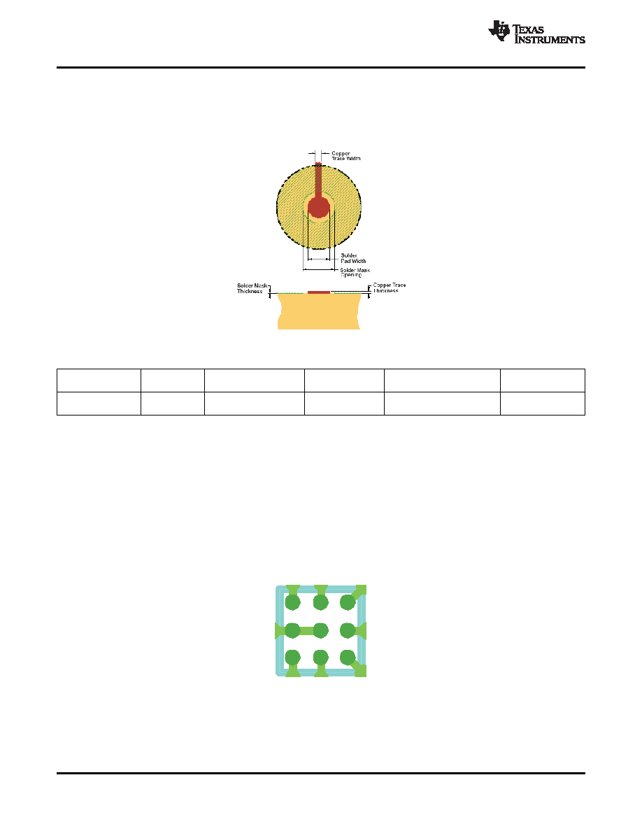
PRINTED CIRCUIT BOARD LAYOUT
In making the pad size for the WCSP balls, it is recommended that the layout use nonsolder mask defined
(NSMD) land. With this method, the solder mask opening is made larger than the desired land area, and the
opening size is defined by the copper pad width. Figure 32 shows the appropriate diameters for a WCSP layout.
Figure 32. Land Pattern Image and Dimensions
SOLDER PAD
SOLDER MASK
COPPER
STENCIL
COPPER PAD
STENCIL OPENING(6)(7)
DEFINITIONS
OPENING(5)
THICKNESS
Nonsolder mask
1 oz max
0.275 mm x 0.275 mm Sq.
0.23 mm
0.310 mm
0.1 mm thick
defined (NSMD)
(0.032 mm)
(rounded corners)
1. Circuit traces from NSMD defined PWB lands should be 75 mm to 100 mm wide in the exposed area inside
the solder mask opening. Wider trace widths reduce device stand off and impact reliability.
2. Best reliability results are achieved when the PWB laminate glass transition temperature is above the
operating the range of the intended application.
3. Recommend solder paste is Type 3 or Type 4.
4. For a PWB using a Ni/Au surface finish, the gold thickness should be less 0.5 mm to avoid a reduction in
thermal fatigue performance.
5. Solder mask thickness should be less than 20 mm on top of the copper circuit pattern
6. Best solder stencil performance is achieved using laser cut stencils with electro polishing. Use of chemically
etched stencils give inferior solder paste volume control.
7. Trace routing away from WCSP device should be balanced in X and Y directions to avoid unintentional
component movement due to solder wetting forces.
Figure 33. Layout Snapshot
An on-pad via is not required to route the middle ball B2 (PVDD) of the TPA2037D1. Just short ball B2 (PVDD) to
ball B1 (VDD) and connect both to the supply trace as shown in Figure 33. This simplifies board routing and
saves manufacturing cost.
14
Copyright 2009–2010, Texas Instruments Incorporated
Product Folder Link(s) : TPA2037D1
相關PDF資料 |
PDF描述 |
|---|---|
| TPA2039D1YFFR | 3.24 W, 1 CHANNEL, AUDIO AMPLIFIER, BGA9 |
| TPA2039D1YFFT | 3.24 W, 1 CHANNEL, AUDIO AMPLIFIER, BGA9 |
| TPA2050D4YZKR | 0.94 W, 2 CHANNEL, AUDIO AMPLIFIER, BGA25 |
| TPA2050D4YZKT | 0.94 W, 2 CHANNEL, AUDIO AMPLIFIER, BGA25 |
| TPA2051D3YFFR | 2.9 W, 2 CHANNEL, AUDIO AMPLIFIER, PBGA25 |
相關代理商/技術參數 |
參數描述 |
|---|---|
| TPA2038D1 | 制造商:TI 制造商全稱:Texas Instruments 功能描述:3.2 W Mono Class-D Audio Power Amplifier With Selectable Gain and Auto-Recovering Short-Circuit Protection |
| TPA2038D1YFFEVM | 功能描述:音頻 IC 開發工具 TPA2038D1 EVAL MOD RoHS:否 制造商:Texas Instruments 產品:Evaluation Kits 類型:Audio Amplifiers 工具用于評估:TAS5614L 工作電源電壓:12 V to 38 V |
| TPA2038D1YFFR | 功能描述:音頻放大器 Variable Gain 3.2W Mono Class-D RoHS:否 制造商:STMicroelectronics 產品:General Purpose Audio Amplifiers 輸出類型:Digital 輸出功率: THD + 噪聲: 工作電源電壓:3.3 V 電源電流: 最大功率耗散: 最大工作溫度: 安裝風格:SMD/SMT 封裝 / 箱體:TQFP-64 封裝:Reel |
| TPA2038D1YFFT | 功能描述:音頻放大器 Variable Gain 3.2W Mono Class-D RoHS:否 制造商:STMicroelectronics 產品:General Purpose Audio Amplifiers 輸出類型:Digital 輸出功率: THD + 噪聲: 工作電源電壓:3.3 V 電源電流: 最大功率耗散: 最大工作溫度: 安裝風格:SMD/SMT 封裝 / 箱體:TQFP-64 封裝:Reel |
| TPA2039D1 | 制造商:TI 制造商全稱:Texas Instruments 功能描述:3.2W Mono Class-D Audio Power Amplifier With 12-dB Gain and Auto Short-Circuit Recovery |
發布緊急采購,3分鐘左右您將得到回復。