- 您現(xiàn)在的位置:買賣IC網(wǎng) > PDF目錄98272 > TPA3100D2IRGZRQ1 (TEXAS INSTRUMENTS INC) 21.8 W, 2 CHANNEL, AUDIO AMPLIFIER, PQCC48 PDF資料下載
參數(shù)資料
| 型號(hào): | TPA3100D2IRGZRQ1 |
| 廠商: | TEXAS INSTRUMENTS INC |
| 元件分類: | 音頻/視頻放大 |
| 英文描述: | 21.8 W, 2 CHANNEL, AUDIO AMPLIFIER, PQCC48 |
| 封裝: | 7 X 7 MM, GREEN, PLASTIC, QFN-48 |
| 文件頁數(shù): | 16/37頁 |
| 文件大小: | 1024K |
| 代理商: | TPA3100D2IRGZRQ1 |
第1頁第2頁第3頁第4頁第5頁第6頁第7頁第8頁第9頁第10頁第11頁第12頁第13頁第14頁第15頁當(dāng)前第16頁第17頁第18頁第19頁第20頁第21頁第22頁第23頁第24頁第25頁第26頁第27頁第28頁第29頁第30頁第31頁第32頁第33頁第34頁第35頁第36頁第37頁
Power-Supply Decoupling, CS
IC Output Snubbers
OUTP
OUTN
1nF
20 W
BSN and BSP Capacitors
VCLAMP Capacitors
Internal Regulated 4-V Supply (VREG)
TPA3100D2-Q1
www.ti.com ......................................................................................................................................................................................... SLOS557 – SEPTEMBER 2008
The TPA3100D2 is a high-performance CMOS audio amplifier that requires adequate power supply decoupling
to ensure that the output total harmonic distortion (THD) is as low as possible. Power supply decoupling also
prevents oscillations for long lead lengths between the amplifier and the speaker. The optimum decoupling is
achieved by using two capacitors of different types that target different types of noise on the power supply leads.
For higher frequency transients, spikes, or digital hash on the line, a good low equivalent-series-resistance (ESR)
ceramic capacitor, typically 0.1
F to 1 F placed as close as possible to the device V
CC lead works best. For
filtering lower frequency noise signals, a larger aluminum electrolytic capacitor of 220
F or greater placed near
the audio power amplifier is recommended. The 220
F capacitor also serves as local storage capacitor for
supplying current during large signal transients on the amplifier outputs. The PVCC terminals provide the power
to the output transistors, so a 220 F or larger capacitor should be placed on each PVCC terminal. A 10 F
capacitor on the AVCC terminal is adequate.
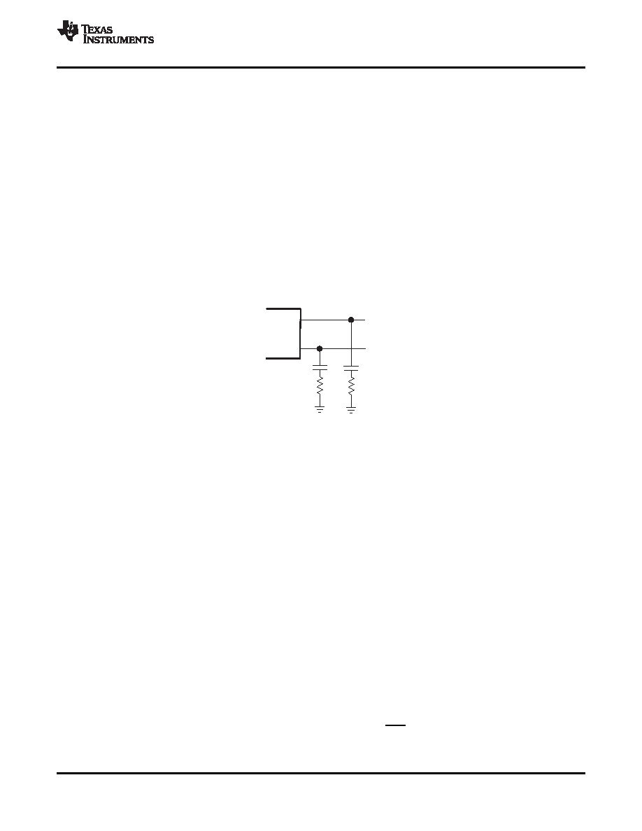
The 1-nF capacitors in series with 20-
Ω resistors from the outputs of the TPA3100D2 IC to ground are switching
snubbers (see Figure 31). They linearize switching transitions and reduce overshoot and ringing. By doing so
they improve THD+N, reducing it by a factor near 3 at 1 kHz and 1 W. They also improve EMC by 2 dB to 6 dB
at middle frequencies. They increase quiescent current by 5 mA to 15 mA, depending on power-supply voltage.
Figure 31. IC Output Snubbers
The full H-bridge output stages use only NMOS transistors. Therefore, they require bootstrap capacitors for the
high side of each output to turn on correctly. A 220-nF ceramic capacitor, rated for at least 25 V, must be
connected from each output to its corresponding bootstrap input. Specifically, one 220-nF capacitor must be
connected from xOUTP to BSxx, and one 220-nF capacitor must be connected from xOUTN to BSxx (see the
application circuit diagram in Figure 21).
The bootstrap capacitors connected between the BSxx pins and corresponding output function as a floating
power supply for the high-side N-channel power MOSFET gate drive circuitry. During each high-side switching
cycle, the bootstrap capacitors hold the gate-to-source voltage high enough to keep the high-side MOSFETs
turned on.
To ensure that the maximum gate-to-source voltage for the NMOS output transistors is not exceeded, two
internal regulators clamp the gate voltage. Two 1-
F capacitors must be connected from VCLAMPL (pin 30) and
VCLAMPR (pin 31) to ground and must be rated for at least 16 V. The voltages at the VCLAMP terminals may
vary with VCC and may not be used for powering any other circuitry.
The VREG terminal (pin 15) is the output of an internally generated 4-V supply, used for the oscillator,
preamplifier, and gain control circuitry. It requires a 10-nF capacitor placed close to the pin to keep the regulator
stable.
This regulated voltage can be used to control GAIN0, GAIN1, MSTR/SLV, and MUTE terminals, but should not
be used to drive external circuitry.
Copyright 2008, Texas Instruments Incorporated
23
相關(guān)PDF資料 |
PDF描述 |
|---|---|
| TPA3100D2RGZR-P | 21.8 W, 2 CHANNEL, AUDIO AMPLIFIER, PQCC48 |
| TPA3100D2RGZR | 21.8 W, 2 CHANNEL, AUDIO AMPLIFIER, PQCC48 |
| TPA3100D2RGZT | 21.8 W, 2 CHANNEL, AUDIO AMPLIFIER, PQCC48 |
| TPA3100D2PHPR | 21.8 W, 2 CHANNEL, AUDIO AMPLIFIER, PQFP48 |
| TPA3100D2RGZRG4 | 21.8 W, 2 CHANNEL, AUDIO AMPLIFIER, PQCC48 |
相關(guān)代理商/技術(shù)參數(shù) |
參數(shù)描述 |
|---|---|
| TPA3100D2PHP | 功能描述:音頻放大器 20 W Stereo Class-D Audio Amp RoHS:否 制造商:STMicroelectronics 產(chǎn)品:General Purpose Audio Amplifiers 輸出類型:Digital 輸出功率: THD + 噪聲: 工作電源電壓:3.3 V 電源電流: 最大功率耗散: 最大工作溫度: 安裝風(fēng)格:SMD/SMT 封裝 / 箱體:TQFP-64 封裝:Reel |
| TPA3100D2PHPG4 | 功能描述:音頻放大器 20 W Stereo Class-D Audio Amp RoHS:否 制造商:STMicroelectronics 產(chǎn)品:General Purpose Audio Amplifiers 輸出類型:Digital 輸出功率: THD + 噪聲: 工作電源電壓:3.3 V 電源電流: 最大功率耗散: 最大工作溫度: 安裝風(fēng)格:SMD/SMT 封裝 / 箱體:TQFP-64 封裝:Reel |
| TPA3100D2PHPR | 功能描述:音頻放大器 20 W Stereo Class-D Audio Amp RoHS:否 制造商:STMicroelectronics 產(chǎn)品:General Purpose Audio Amplifiers 輸出類型:Digital 輸出功率: THD + 噪聲: 工作電源電壓:3.3 V 電源電流: 最大功率耗散: 最大工作溫度: 安裝風(fēng)格:SMD/SMT 封裝 / 箱體:TQFP-64 封裝:Reel |
| TPA3100D2PHPRG4 | 功能描述:音頻放大器 20 W Stereo Class-D Audio Amp RoHS:否 制造商:STMicroelectronics 產(chǎn)品:General Purpose Audio Amplifiers 輸出類型:Digital 輸出功率: THD + 噪聲: 工作電源電壓:3.3 V 電源電流: 最大功率耗散: 最大工作溫度: 安裝風(fēng)格:SMD/SMT 封裝 / 箱體:TQFP-64 封裝:Reel |
| TPA3100D2-Q1 | 制造商:TI 制造商全稱:Texas Instruments 功能描述:20-W STEREO CLASS-D AUDIO POWER AMPLIFIER |
發(fā)布緊急采購,3分鐘左右您將得到回復(fù)。