- 您現在的位置:買賣IC網 > PDF目錄98280 > TPS24710DGS (TEXAS INSTRUMENTS INC) POWER SUPPLY SUPPORT CKT, PDSO10 PDF資料下載
參數資料
| 型號: | TPS24710DGS |
| 廠商: | TEXAS INSTRUMENTS INC |
| 元件分類: | 電源管理 |
| 英文描述: | POWER SUPPLY SUPPORT CKT, PDSO10 |
| 封裝: | GREEN, PLASTIC, MSOP-10 |
| 文件頁數: | 18/34頁 |
| 文件大小: | 2148K |
| 代理商: | TPS24710DGS |
第1頁第2頁第3頁第4頁第5頁第6頁第7頁第8頁第9頁第10頁第11頁第12頁第13頁第14頁第15頁第16頁第17頁當前第18頁第19頁第20頁第21頁第22頁第23頁第24頁第25頁第26頁第27頁第28頁第29頁第30頁第31頁第32頁第33頁第34頁
G009
1k
10
0.01
1
100
I
–
D
ra
in
-t
o
-So
u
rce
C
u
rre
n
t
–
A
D
S
0.1
0.01
0.1
10
100
1
Single Pulse
R
= 94C/W (min Cu)
θ
JA
1ms
10ms
100ms
1s
DC
Area Limited
by R
DS(on)
V
– Drain-to-Source Voltage – V
DS
2
ENTHRESH
VCC
1
2
R
V
R
=
+
OUT
VCC
CHG
C
V
t
I
D =
SLVSAL2C
– JANUARY 2011 – REVISED MAY 2011
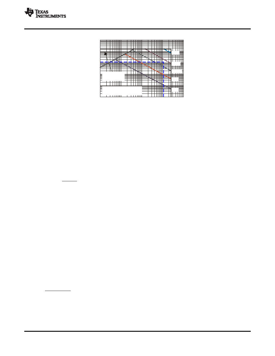
Figure 35. CSD16403Q5 SOA Curve
STEP 5. Calculate the Retry-Mode Duty Ratio
In retry mode, the TPS24711/13 is on for one charging cycle and off for 16 charge/discharge cycles, as can be
seen in Figure 32. The first CT charging cycle is from 0 V to 1.35 V, which gives 7.56 ms. The first CT discharging
cycle is from 1.35 V to 0.35 V, which gives 5.6 ms. Therefore, the total time is 7.56 ms + 33
× 5.6 ms = 192.36
ms. As a result, the retry mode duty ratio is 7.56 ms/192.36 ms = 3.93%.
STEP 6. Select R1 and R2 for UV
Next, select the values of the UV resistors, R1 and R2, as shown in the typical application diagram on the front
page. From the TPS24710/11/12/13 electrical specifications, VENTHRESH = 1.35 V. The VUV is the undervoltage
trip voltage, which for this example equals 10.7 V.
(12)
STEP 7. Choose RGATE, R4, R5 and C1
In the typical application diagram on the front page, the gate resistor, RGATE, is intended to suppress
high-frequency oscillations. A resistor of 10
Ω will serve for most applications, but if M1 has a CISS below 200 pF,
then 33
Ω is recommended. Applications with larger MOSFETs and very short wiring may not require RGATE. R4
and R5 are required only if PGb and FLTb are used; these resistors serve as pullups for the open-drain output
drivers. The current sunk by each of these pins should not exceed 2 mA (see the RECOMMENDED
OPERATING CONDITIONS table). C1 is a bypass capacitor to help control transient voltages, unit emissions,
and local supply noise while in the disabled state. Where acceptable, a value in the range of 0.001
μF to 0.1 μF
is recommended.
ALTERNATIVE DESIGN EXAMPLE: GATE CAPACITOR (dV/dt) CONTROL IN INRUSH MODE
The TPS24710/11/12/13 can be used in applications that expect a constant inrush current. This current is
controlled by a capacitor connected from the GATE terminal to GND. A resistor of 1 k
placed in series with this
capacitor will prevent it from slowing a fast-turnoff event. In this mode of operation, M1 operates as a source
follower, and the slew rate of the output voltage approximately equals the slew rate of the gate voltage (see
To implement a constant-inrush-current circuit, choose the time to charge,
t, using Equation 13,
(13)
where COUT is the output capacitance, VVCC is the input voltage, and ICHG is the desired charge current. Set PLIM
to a value greater than VVCC × ICHG to prevent power limiting from affecting the desired current.
To select the gate capacitance, use Equation 14.
Copyright
2011, Texas Instruments Incorporated
25
相關PDF資料 |
PDF描述 |
|---|---|
| TPS24710 | POWER SUPPLY SUPPORT CKT, PDSO10 |
| TPS24711 | POWER SUPPLY SUPPORT CKT, PDSO10 |
| TPS24711DGSR | POWER SUPPLY SUPPORT CKT, PDSO10 |
| TPS2481PW | POWER SUPPLY SUPPORT CKT, PDSO20 |
| TPS2480PW | POWER SUPPLY SUPPORT CKT, PDSO20 |
相關代理商/技術參數 |
參數描述 |
|---|---|
| TPS24710DGSR | 功能描述:熱插拔功率分布 2.5-18V Hi Eff Hot- Swap Controller RoHS:否 制造商:Texas Instruments 產品:Controllers & Switches 電流限制: 電源電壓-最大:7 V 電源電壓-最小:- 0.3 V 工作溫度范圍: 功率耗散: 安裝風格:SMD/SMT 封裝 / 箱體:MSOP-8 封裝:Tube |
| TPS24710EVM-003 | 功能描述:電源管理IC開發工具 TPS24710 Eval Mod RoHS:否 制造商:Maxim Integrated 產品:Evaluation Kits 類型:Battery Management 工具用于評估:MAX17710GB 輸入電壓: 輸出電壓:1.8 V |
| TPS24711DGS | 功能描述:熱插拔功率分布 2.5-18V Hi Eff Hot- Swap Controller RoHS:否 制造商:Texas Instruments 產品:Controllers & Switches 電流限制: 電源電壓-最大:7 V 電源電壓-最小:- 0.3 V 工作溫度范圍: 功率耗散: 安裝風格:SMD/SMT 封裝 / 箱體:MSOP-8 封裝:Tube |
| TPS24711DGSR | 功能描述:熱插拔功率分布 2.5-18V Hi Eff Hot- Swap Controller RoHS:否 制造商:Texas Instruments 產品:Controllers & Switches 電流限制: 電源電壓-最大:7 V 電源電壓-最小:- 0.3 V 工作溫度范圍: 功率耗散: 安裝風格:SMD/SMT 封裝 / 箱體:MSOP-8 封裝:Tube |
| TPS24711EVM-004 | 功能描述:電源管理IC開發工具 TPS24711 Eval Mod RoHS:否 制造商:Maxim Integrated 產品:Evaluation Kits 類型:Battery Management 工具用于評估:MAX17710GB 輸入電壓: 輸出電壓:1.8 V |
發布緊急采購,3分鐘左右您將得到回復。