- 您現(xiàn)在的位置:買賣IC網(wǎng) > PDF目錄98281 > TPS5120QDBTRQ1 (TEXAS INSTRUMENTS INC) 1.5 A DUAL SWITCHING CONTROLLER, 500 kHz SWITCHING FREQ-MAX, PDSO30 PDF資料下載
參數(shù)資料
| 型號: | TPS5120QDBTRQ1 |
| 廠商: | TEXAS INSTRUMENTS INC |
| 元件分類: | 穩(wěn)壓器 |
| 英文描述: | 1.5 A DUAL SWITCHING CONTROLLER, 500 kHz SWITCHING FREQ-MAX, PDSO30 |
| 封裝: | PLASTIC, SM8-30 |
| 文件頁數(shù): | 16/21頁 |
| 文件大小: | 320K |
| 代理商: | TPS5120QDBTRQ1 |
TPS5120Q1
DUAL OUTPUT, TWOPHASE SYNCHRONOUS BUCK DC/DC CONTROLLER
SGLS225B JANUARY 2004 REVISED APRIL 2008
4
POST OFFICE BOX 655303
DALLAS, TEXAS 75265
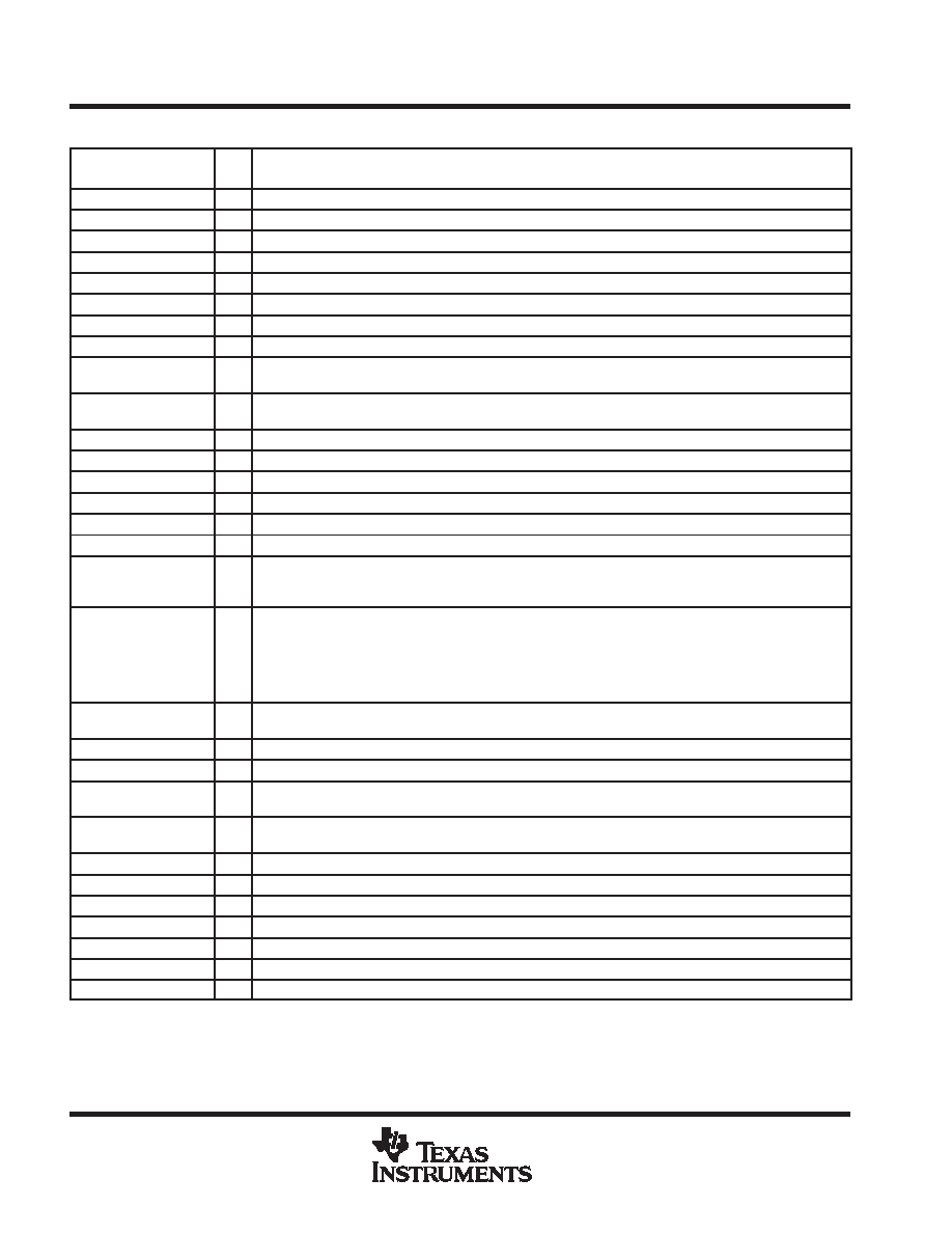
Terminal Functions
TERMINAL
I/O
DESCRIPTION
NAME
NO.
I/O
DESCRIPTION
CT
5
I/O
External capacitor from CT to GND for adjusting the triangle oscillator
FB1
2
O
Feedback output of CH1 error amplifier
FB2
14
O
Feedback output of CH2 error amplifier
GND
7
Control GND
INV1
1
I
Inverting input of the CH1 error amplifier, skip comparator, and OVP1/UVP1 comparator
INV2
15
I
Inverting input of the CH2 error amplifier, skip comparator, and OVP2/UVP2 comparator
LH1
30
I/O
Bootstrap capacitor connection for CH1 high-side gate drive
LH2
16
I/O
Bootstrap capacitor connection for CH2 high-side gate drive
LL1
28
I/O
Bootstrap this pin low for CH1 high-side gate driving return and output current protection. Connect this pin to
the junction of the high-side and low-side FETs for a floating drive configuration.
LL2
18
I/O
Bootstrap this pin low for CH2 high-side gate driving return and output current protection. Connect this pin to
the junction of the high-side and low-side FETs for a floating drive configuration.
OUT1_d
27
O
Gate drive output for CH1 low-side gate drive
OUT2_d
19
O
Gate drive output for CH2 low-side gate drive
OUT1_u
29
O
Gate drive output for CH1 high-side switching FETs
OUT2_u
17
O
Gate drive output for CH2 high-side switching FETs
OUTGND1
26
Ground for CH1 FET drivers
OUTGND2
20
Ground for CH2 FET drivers
POWERGOOD
12
O
Power good open-drain output. When low, POWERGOOD reports an output fail condition. PG comparators
monitor both SMPS’s over voltage and UVLO of VREF5. The threshold is
±7%. When the SMPS starts up, the
POWERGOOD pin’s output goes high. POWERGOOD also monitors VREF5’s UVLO output.
PWM/SKIP
4
I
PWM/SKIP mode select pin. The PWM/SKIP pin is used to change the output’s operating mode. If this terminal
is lower than 0.5 V, it works in PWM mode. When a minimum voltage of 2 V is applied, the device operates in
skip mode. In light load condition (< 0.2 A), the skip mode gives a short pulse to the low-side FETs instead of a
full pulse. With this control, switching frequency is lowered and switching loss is reduced. Also, the output
capacitor energy discharging through the output inductor and low-side FETs is stopped. Therefore, TPS5120
achieves a higher efficiency in light load conditions.
REF
8
O
0.85-V reference voltage output. The 0.85-V reference voltage is used for setting the output voltage and the
voltage protection. This reference voltage is dropped down from a 5-V regulator.
REG5V_IN
21
I
External 5-V input
FLT
11
I/O
Fault latch timer pin. An external capacitor is connected between FLT and GND to set the FLT enable time up.
SOFTSTART1
3
I/O
External capacitor from SOFTSTART1 to GND for CH1 softstart control. Separate soft-start terminals make it
possible to set the start-up time of each output independently.
SOFTSTART2
13
I/O
External capacitor from SOFTSTART2 to GND for CH2 softstart control. Separate soft-start terminals make it
possible to set the start-up time of each output independently.
STBY1
9
I
Standby control for CH1. SMPS1 can be switched into standby mode separately by grounding the STBY1 pin.
STBY2
10
I
Standby control for CH2. SMPS2 can be switched into standby mode separately by grounding the STBY2 pin.
TRIP1
25
I
External resistor connection for CH1 output current control
TRIP2
23
I
External resistor connection for CH2 output current control
VCC
24
Supply voltage input
VREF5
22
O
5-V internal regulator output
5V_STBY
6
I
5-V linear regulator control
相關(guān)PDF資料 |
PDF描述 |
|---|---|
| TPS51211DSCT | SWITCHING CONTROLLER, 314 kHz SWITCHING FREQ-MAX, PDSO10 |
| TPS51211DSCR | SWITCHING CONTROLLER, 314 kHz SWITCHING FREQ-MAX, PDSO10 |
| TPS51220ARTVR | DUAL SWITCHING CONTROLLER, 333 kHz SWITCHING FREQ-MAX, PQCC32 |
| TPS51221RTVRG4 | DUAL SWITCHING CONTROLLER, 333 kHz SWITCHING FREQ-MAX, PQCC32 |
| TPS51315RGFR | SWITCHING REGULATOR, 1000 kHz SWITCHING FREQ-MAX, PQCC40 |
相關(guān)代理商/技術(shù)參數(shù) |
參數(shù)描述 |
|---|---|
| TPS5120QDBTRQ1G4 | 功能描述:DC/DC 開關(guān)控制器 Dual Out 2Ph Synch Buck DC/DC Cntrlr RoHS:否 制造商:Texas Instruments 輸入電壓:6 V to 100 V 開關(guān)頻率: 輸出電壓:1.215 V to 80 V 輸出電流:3.5 A 輸出端數(shù)量:1 最大工作溫度:+ 125 C 安裝風(fēng)格: 封裝 / 箱體:CPAK |
| TPS5120QDBTRRB | 制造商:Texas Instruments 功能描述:ENHANCED PRODUCT DUAL O/P CONTROLLER |
| TPS51211 | 制造商:TI 制造商全稱:Texas Instruments 功能描述:HIGH PERFORMANCE, SINGLE SYNCHRONOUS STEP-DOWN CONTROLLER FOR NOTEBOOK POWER SUPPLY |
| TPS51211DSCR | 功能描述:DC/DC 開關(guān)控制器 Hi-Perf,Single Synch Step-Down Controller RoHS:否 制造商:Texas Instruments 輸入電壓:6 V to 100 V 開關(guān)頻率: 輸出電壓:1.215 V to 80 V 輸出電流:3.5 A 輸出端數(shù)量:1 最大工作溫度:+ 125 C 安裝風(fēng)格: 封裝 / 箱體:CPAK |
| TPS51211DSCT | 功能描述:DC/DC 開關(guān)控制器 Hi-Perf,Single Synch Step-Down Controller RoHS:否 制造商:Texas Instruments 輸入電壓:6 V to 100 V 開關(guān)頻率: 輸出電壓:1.215 V to 80 V 輸出電流:3.5 A 輸出端數(shù)量:1 最大工作溫度:+ 125 C 安裝風(fēng)格: 封裝 / 箱體:CPAK |
發(fā)布緊急采購,3分鐘左右您將得到回復(fù)。