- 您現在的位置:買賣IC網 > PDF目錄382679 > TPS54672PWP Analog IC PDF資料下載
參數資料
| 型號: | TPS54672PWP |
| 英文描述: | Analog IC |
| 中文描述: | 模擬IC |
| 文件頁數: | 4/16頁 |
| 文件大小: | 260K |
| 代理商: | TPS54672PWP |
TPS54611, TPS54612, TPS54613
TPS54614, TPS54615, TPS54616
SLVS400A
–
AUGUST 2001
–
REVISED JANUARY 2002
4
www.ti.com
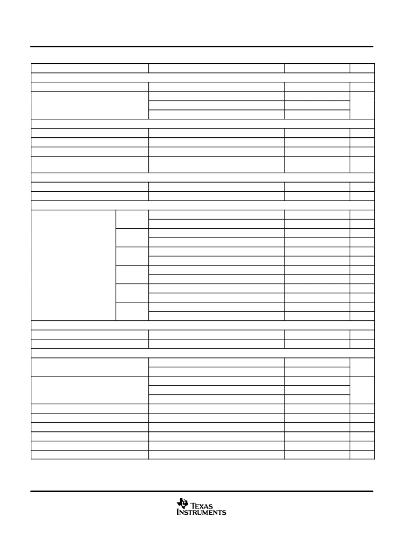
electrical characteristics, T
J
=
–
40
°
C to 125
°
C, V
I
= 3 V to 6 V (unless otherwise noted)
PARAMETER
TEST CONDITIONS
MIN
TYP
MAX
UNIT
SUPPLY VOLTAGE, VIN
Input voltage range, VIN
3.0
6.0
V
fs = 350 kHz, FSEL
≤
0.8 V, RT open, phase pin open
fs = 550 kHz, FSEL
≤
2.5 V, RT open, phase pin open
Shutdown, SS/ENA = 0 V
6.2
9.6
I(Q)
Quiescent current
8.4
12.8
mA
1
1.4
UNDER VOLTAGE LOCK OUT
Start threshold voltage, UVLO
2.95
3.0
V
Stop threshold voltage, UVLO
2.70
2.80
V
Hysteresis voltage, UVLO
0.14
0.16
V
Rising and falling edge deglitch,
UVLO
See Note 1
2.5
μ
s
BIAS VOLTAGE
Output voltage, VBIAS
I(VBIAS) = 0
See Note 2
2.70
2.80
2.90
V
μ
A
Output current, VBIAS
100
OUTPUT VOLTAGE
TPS54611
TJ = 25
°
C, VIN = 5 V
3 V
≤
VIN
≤
6 V, 0
≤
IL
≤
6 A,
–
40
°
≤
TJ
≤
125
°
C
TJ = 25
°
C, VIN = 5 V
3 V
≤
VIN
≤
6 V, 0
≤
IL
≤
6 A,
–
40
°
≤
TJ
≤
125
°
C
TJ = 25
°
C, VIN = 5 V
3 V
≤
VIN
≤
6 V, 0
≤
IL
≤
6 A,
–
40
°
≤
TJ
≤
125
°
C
TJ = 25
°
C, VIN = 5 V
3 V
≤
VIN
≤
6 V, 0
≤
IL
≤
6 A,
–
40
°
≤
TJ
≤
125
°
C
TJ = 25
°
C, VIN = 5 V
3 V
≤
VIN
≤
6 V, 0
≤
IL
≤
6 A,
–
40
°
≤
TJ
≤
125
°
C
TJ = 25
°
C, VIN = 5 V
3 V
≤
VIN
≤
6 V, 0
≤
IL
≤
6 A,
–
40
°
≤
TJ
≤
125
°
C
0.9
V
–
2.0%
2.0%
TPS54612
1.2
V
–
2.0%
2.0%
TPS54613
1.5
V
VO
Output voltage
–
2.0%
2.0%
TPS54614
1.8
V
–
3.0%
3.0%
TPS54615
2.5
V
–
3.0%
3.0%
TPS54616
3.3
V
–
3.0%
3.0%
REGULATION
Line regulation (see Notes 1 and 3)
IL = 3 A, 350
≤
fs
≤
550 kHz, TJ = 85
°
C
IL = 0 A to 6 A, 350
≤
fs
≤
550 kHz, TJ = 85
°
C
0.088
%/V
Load regulation (see Notes 1 and 3)
0.0917
%/A
OSCILLATOR
—
Internally set
frequency
SYNC
≤
0.8 V,
SYNC
≥
2.5 V,
RT = 180 k
(1% resistor to AGND)
RT = 100 k
(1% resistor to AGND)
RT = 68 k
(1% resistor to AGND)
RT open
280
350
420
kHz
free running
RT open
440
550
660
E t
Externally set
—
free running
frequency range
252
280
308
460
500
540
kHz
280
700
762
High level threshold, FSEL
2.5
V
Low level threshold, FSEL
0.8
V
Ramp valley
See Note 1
0.75
V
Ramp amplitude (peak-to-peak)
See Note 1
1
V
Minimum controllable on time
See Note 1
200
ns
Maximum duty cycle
1. Specified by design
2. Static resistive loads only
3. Tested using circuit in Figure 10.
See Note 1
90%
NOTES:
相關PDF資料 |
PDF描述 |
|---|---|
| TPS54672PWPR | Analog IC |
| TPS54673PWP | SMPS Controller |
| TPS54673PWPR | SMPS Controller |
| TPS54680PWPR | SMPS Controller |
| TPS54311PWPR | Analog IC |
相關代理商/技術參數 |
參數描述 |
|---|---|
| TPS54672PWPG4 | 功能描述:直流/直流開關調節器 6-A Act Bus Term/DDR DC/DC Converter RoHS:否 制造商:International Rectifier 最大輸入電壓:21 V 開關頻率:1.5 MHz 輸出電壓:0.5 V to 0.86 V 輸出電流:4 A 輸出端數量: 最大工作溫度: 安裝風格:SMD/SMT 封裝 / 箱體:PQFN 4 x 5 |
| TPS54672PWPR | 功能描述:直流/直流開關調節器 6-A Act Bus Term/DDR DC/DC Converter RoHS:否 制造商:International Rectifier 最大輸入電壓:21 V 開關頻率:1.5 MHz 輸出電壓:0.5 V to 0.86 V 輸出電流:4 A 輸出端數量: 最大工作溫度: 安裝風格:SMD/SMT 封裝 / 箱體:PQFN 4 x 5 |
| TPS54672PWPR | 制造商:Texas Instruments 功能描述:IC SYNC PWM SWITCHER |
| TPS54672PWPRG4 | 功能描述:直流/直流開關調節器 6-A Act Bus Term/DDR DC/DC Converter RoHS:否 制造商:International Rectifier 最大輸入電壓:21 V 開關頻率:1.5 MHz 輸出電壓:0.5 V to 0.86 V 輸出電流:4 A 輸出端數量: 最大工作溫度: 安裝風格:SMD/SMT 封裝 / 箱體:PQFN 4 x 5 |
| TPS54672PWRG4 | 制造商:Texas Instruments 功能描述: |
發布緊急采購,3分鐘左右您將得到回復。