- 您現(xiàn)在的位置:買賣IC網(wǎng) > PDF目錄98284 > TPS61221DCKR (TEXAS INSTRUMENTS INC) 0.4 A BATTERY CHARGE CONTROLLER, PDSO6 PDF資料下載
參數(shù)資料
| 型號: | TPS61221DCKR |
| 廠商: | TEXAS INSTRUMENTS INC |
| 元件分類: | 穩(wěn)壓器 |
| 英文描述: | 0.4 A BATTERY CHARGE CONTROLLER, PDSO6 |
| 封裝: | GREEN, PLASTIC, SC-70, 6 PIN |
| 文件頁數(shù): | 7/22頁 |
| 文件大小: | 1333K |
| 代理商: | TPS61221DCKR |
2
L
C
2
(5)
Layout Considerations
V
IN
V
OUT
GND
L1
C1
C2
R1
R2
GND
Enable
V
IN
V
O
U
T
www.ti.com ............................................................................................................................................................................................... SLVS776 – JANUARY 2009
A minimum capacitance value of 4.7
F should be used, 10 F are recommended. If the inductor value exceeds
4.7
H, the value of the output capacitance value needs to be half the inductance value or higher for stability
reasons, see Equation 5.
The TPS6122x is not sensitive to the ESR in terms of stability. Using low ESR capacitors, such as ceramic
capacitors, is recommended anyway to minimize output voltage ripple. If heavy load changes are expected, the
output capacitor value should be increased to avoid output voltage drops during fast load transients.
As for all switching power supplies, the layout is an important step in the design, especially at high peak currents
and high switching frequencies. If the layout is not carefully done, the regulator could show stability problems as
well as EMI problems. Therefore, use wide and short traces for the main current path and for the power ground
paths. The input and output capacitor, as well as the inductor should be placed as close as possible to the IC.
The feedback divider should be placed as close as possible to the control ground pin of the IC. To lay out the
ground, it is recommended to use short traces as well, separated from the power ground traces. This avoids
ground shift problems, which can occur due to superimposition of power ground current and control ground
current. Assure that the ground traces are connected close to the device GND pin.
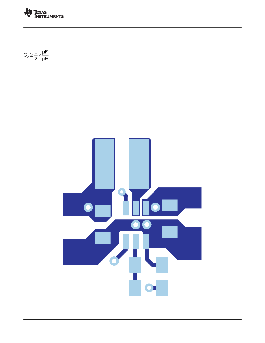
Figure 26. PCB Layout Suggestion for Adjustable Output Voltage Options
Copyright 2009, Texas Instruments Incorporated
15
Product Folder Link(s): TPS61220 TPS61221 TPS61222
相關(guān)PDF資料 |
PDF描述 |
|---|---|
| TPS61251DSGT | SWITCHING REGULATOR, 3500 kHz SWITCHING FREQ-MAX, PDSO8 |
| TPS61251DSG | SWITCHING REGULATOR, 3500 kHz SWITCHING FREQ-MAX, PDSO8 |
| TPS62000YEGR | 1.6 A SWITCHING REGULATOR, 1000 kHz SWITCHING FREQ-MAX, BGA12 |
| TPS62000YEGT | 1.6 A SWITCHING REGULATOR, 1000 kHz SWITCHING FREQ-MAX, BGA12 |
| TPS62000YEG | 1.6 A SWITCHING REGULATOR, 1000 kHz SWITCHING FREQ-MAX, BGA12 |
相關(guān)代理商/技術(shù)參數(shù) |
參數(shù)描述 |
|---|---|
| TPS61221DCKT | 功能描述:直流/直流開關(guān)調(diào)節(jié)器 Tiny Low Inp Vltg Boost Cnvrtr RoHS:否 制造商:International Rectifier 最大輸入電壓:21 V 開關(guān)頻率:1.5 MHz 輸出電壓:0.5 V to 0.86 V 輸出電流:4 A 輸出端數(shù)量: 最大工作溫度: 安裝風格:SMD/SMT 封裝 / 箱體:PQFN 4 x 5 |
| TPS61222DCKR | 功能描述:直流/直流開關(guān)調(diào)節(jié)器 Tiny Low Inp Vltg Boost Cnvrtr RoHS:否 制造商:International Rectifier 最大輸入電壓:21 V 開關(guān)頻率:1.5 MHz 輸出電壓:0.5 V to 0.86 V 輸出電流:4 A 輸出端數(shù)量: 最大工作溫度: 安裝風格:SMD/SMT 封裝 / 箱體:PQFN 4 x 5 |
| TPS61222DCKT | 功能描述:直流/直流開關(guān)調(diào)節(jié)器 Tiny Low Inp Vltg Boost Cnvrtr RoHS:否 制造商:International Rectifier 最大輸入電壓:21 V 開關(guān)頻率:1.5 MHz 輸出電壓:0.5 V to 0.86 V 輸出電流:4 A 輸出端數(shù)量: 最大工作溫度: 安裝風格:SMD/SMT 封裝 / 箱體:PQFN 4 x 5 |
| TPS61222MDCKTEP | 功能描述:直流/直流開關(guān)轉(zhuǎn)換器 Boost Converter with 5.5?A Quiescnt Crrnt RoHS:否 制造商:STMicroelectronics 最大輸入電壓:4.5 V 開關(guān)頻率:1.5 MHz 輸出電壓:4.6 V 輸出電流:250 mA 輸出端數(shù)量:2 最大工作溫度:+ 85 C 安裝風格:SMD/SMT |
| TPS61223DCKR | 制造商:Texas Instruments 功能描述: |
發(fā)布緊急采購,3分鐘左右您將得到回復。